This thread has been locked.

If you have a related question, please click the "Ask a related question" button in the top right corner. The newly created question will be automatically linked to this question.

TMS320F280049: Glitch on ADC Sample

Part Number: TMS320F280049

Hi Team,

My customer is reaching out to me on a glitch that they observed on the F280049 ADC. Below is the waveform captured by customer:
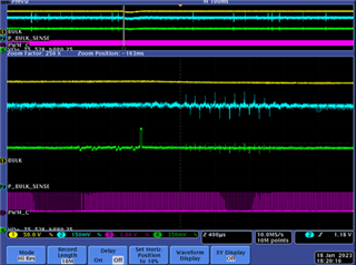
Blue is the signal to the ADC, measured from MCU pin.
Green is DAC output of the same signal.

Can you share any design guides to kill the high frequency noise from SnH/ADC, if you have any.
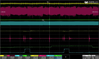
Noise is observed in the ADCpin. But not before signal buffer.

Thanks!

BR,
Alfred

  • Hi Team,

    An additional question from customer relating to above post.

    We your need your help in analyzing the ADC sample issue.

    Blue    - PWM pulses

    Red     - Input Signal

    Green – Replicated input signal using ADC and DAC as monitoring signal

    We are getting a bump(Green) from the sampled signal (RED).

    This can be due to glitches, however the glitch are very high frequency,

    See the orange indicator. That is the point of sample and hold.

    Can the glitch be captured by the S&H and ADC?

    Thanks!

    BR,

    Alfred

  • Hello Alfred,

    First to the question of how to design to deal with noise in the ADC sampling circuit: I recommend referring to our application notes on ADC input driver design. Proper driver circuit design is important to achieving ADC performance.

    These are also linked to at the beginnig of the ADC chapter in the device technical reference manual.

    In addition, you want to also ensure that your VREFHI pin has sufficient decoupling capacitance. At a minimum, you should have at least 2.2uF of decap on the VREFHI pin. If using external VREF mode, we recommend using a high quality series reference as well; this is covered in more detail in the device TRM under ADC > Additional Information > Designing an External Reference Circuit. Also make sure you have decoupling capacitance on the VDDA pin, and if you are sharing a power rail with the VDDIO supply, you might consider using a ferrite bead to gain some noise isolation.

    Specifically to this problem:

    • Yes, it is possible for the ADC to sample a glitch on the input. The question would be -- does the amplitude of the glitch correlate to the conversion result, and is the glitch width similar to the acquisition window duration (ACQPS)?
    • Some basics:
      • Ensure that ADCCTL2.PRESCALE (the ADCCLK divider) is configured to 2 (50MHz from 100MHz SYSCLK). ADC will not function correctly if PRESCALE is set too low. Do not use fractional values as these can degrade performance (noted in errata document).
      • Ensure that you have configured ACQPS to a minimum of 7 (80 ns on 100MHz SYSCLK)
      • If you are using DMA to read the ADC results, you may read a stale ADC result from say a different SOC. This is also noted in the device errata; the workaround is to trigger two different DMA channels and use the second channel to read.

    Hope the above suggestions are helpful!

    Ibukun

  • Hi Ibukun,

    Thanks for the feedback! Please see below feedback from customer:


    Layout and component related was carefully considered during the early stages.

    No DMA used, 50Mhz ADC clock settings.


    Current ACQPS value is 20, which I copied from old sample.

    Reducing ACQPS will probably move the sampling away from noise sources.

    We will try this today.

    Thanks!

    BR,

    Alfred

  • Thanks Alfred, will await the results. Please also share if they are using DMA (and there are other SOCs/channels configured for this ADC).

  • Hi Ibukun,

    Got feedback from customer, there is no DMA implemented, for the ADC.

    3ADC by 4 samples. Problematic sample is the fourth.

    Thanks!

    BR,

    Alfred

  • Alfred,

    I would like to attempt to reproduce this scenario in the lab. Please ask customer to provide some details on the SOC configuration for all ADCs (trigger source, SOCs configured, ACQPS, channel #, what priority).

    If I understand correctly, they are sampling all 3 ADCs simultaneously (on different channels I assume), and then the first ADC shows a glitch when it gets to its second sample?

    Thanks,
    Ibukun

  • Hi Ibukun,

    I am asking customer for this info and will share with you. Customer does have some clarifications:

    Please see attached file.


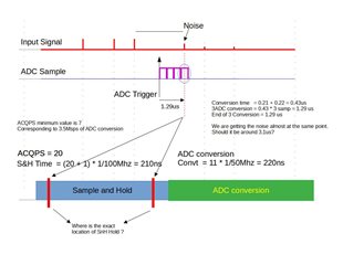
    For the ADC conversion can we assume 10.5 or 11  clock cycles?

    For the SnH Capture point, is it 5ns before start of conversion?

    Thanks !

    BR,

    Alfred

  • Alfred,

    Details of ADC timings are specified in the "ADC Timings" section of the device technical reference manual. There is no single "capture point" for sample and hold, the entire ACQPS window is used to pre-charge the sample capacitor. The conversion period begins immediately after the S+H period, and the total conversion time will always be a whole number of SYSCLK cycles - so if conversion takes 10.5 ADCCLK cycles, with a prescale of 2 that would translate to 21 SYSCLK cycles. Note that the ADC interrupt timing does not coincide with EOC either. For exact timing numbers the customer should always refer to the data in the TRM.

    Best regards,
    Ibukun