This thread has been locked.

If you have a related question, please click the "Ask a related question" button in the top right corner. The newly created question will be automatically linked to this question.

TMDSCNCD28335: F28335 SPI Conmmunication between Two F28335 Device

Part Number: TMDSCNCD28335
Other Parts Discussed in Thread: TMDSDOCK28335

Hi team,

I help my customer to ask a question.

"

I am trying to get started with the SPI function on F28335. Right now, I am using two TMDSCNCD28335 control cards with docking stations. As I am trying to start, I am planning to use board 1 as the master device in SPI, and use board 2 as the slave device. Device 1 will send the time data with the second unit to device 2. Device 2 will only send the dummy data of 0xF to device 1. For my dissertation project, I am using the ADC interrupt triggered by EPWMSOCA instead of the SPI interrupts. I modified the demo code from the control suite to achieve this task. But it looks the data received by device 1/2 are all random values instead of the value I loaded into transmitter buffers. Here is my partial code for SPI:


DEVICE #1

void InitSpiFifoMaster()
{
	/*Initializa SPI Slave Mode without FIFO*/
	SpiaRegs.SPICCR.bit.SPISWRESET = 0; 		// Reset SPI
	
	SpiaRegs.SPICCR.bit.SPICHAR = 0xF;			// Set SPI charater length to be 16-bit (0xF)
	SpiaRegs.SPICTL.bit.MASTER_SLAVE = 1;		// Master->1, Slave->0
	SpiaRegs.SPICTL.bit.TALK = 1;				// Transmit Enable. Set as 0 will disable TX for next word by set output line HIGH
	SpiaRegs.SPIBRR = 0x0063;           		// Set baud rate: 40MHz/(0x63+0x1)=40MHz/100=400bps
	SpiaRegs.SPIPRI.bit.FREE = 1;				// Enable Free Run, continure SPI operation no matter the suspend occurred
	/*Set SPI FIFO Regs*/
	SpiaRegs.SPIFFTX.bit.SPIRST = 1;			// SPI Reset, SPI FIFO can resume transmit/receive
	SpiaRegs.SPIFFTX.bit.SPIFFENA = 1;			// SPI FIFO Enable
	SpiaRegs.SPIFFTX.bit.TXFIFO = 1;			// TX FIFO Release from reset mode
	SpiaRegs.SPIFFTX.bit.TXFFINTCLR = 1;		// Clear TXFIFO Interrupt (W1C: Write on to clear)
	SpiaRegs.SPIFFTX.bit.TXFFIL = 0x00;			// Set TX FIFO Interrupt Level to be 0
	SpiaRegs.SPIFFRX.bit.RXFIFORESET = 1;		// Release Receive FIFO from reset mode
	SpiaRegs.SPIFFRX.bit.RXFFINTCLR = 1;		// Clear SPI FIFO RXFFINTCLR flag (W1C: write one to clear)
	SpiaRegs.SPIFFRX.bit.RXFFIL = 0x0;			// Set RX FIFO Interrupt Level to be 0
	SpiaRegs.SPIFFCT.bit.TXDLY = 0x00;			// FIFO transmit delay to be zero

	SpiaRegs.SPICCR.bit.SPISWRESET=1;  			// Release SPI from reset mode
}

void SpiTxDat(Uint16 tx)
{
	/*MASTER SEND TIME TO SLAVE*/
	GpioDataRegs.GPACLEAR.bit.GPIO19 = 1;
	SpiaRegs.SPITXBUF = tx;						// Load data to SPI Output Buffer
	while(SpiaRegs.SPIFFRX.bit.RXFFST != 1);	// Wait until data is received
	DataSpiRx = SpiaRegs.SPIRXBUF;				// Read received data
	GpioDataRegs.GPASET.bit.GPIO19 = 1;
}


DEVICE #2

void InitSpiFifoSlave()
{
	/*Initializa SPI Slave Mode without FIFO*/
	SpiaRegs.SPICCR.bit.SPISWRESET = 0; 		// Reset SPI
	
	SpiaRegs.SPICCR.bit.SPICHAR = 0xF;			// Set SPI charater length to be 16-bit (0xF)
	SpiaRegs.SPICTL.bit.MASTER_SLAVE = 0;		// Master->1, Slave->0
	SpiaRegs.SPICTL.bit.TALK = 1;				// Transmit Enable. Set as 0 will disable TX for next word by set output line HIGH
	SpiaRegs.SPIBRR = 0x0063;           		// Set baud rate: 40MHz/(0x63+0x1)=40MHz/100=400bps
	SpiaRegs.SPIPRI.bit.FREE = 1;				// Enable Free Run, continure SPI operation no matter the suspend occurred
	/*Set SPI FIFO Regs*/
	SpiaRegs.SPIFFTX.bit.SPIRST = 1;			// SPI Reset, SPI FIFO can resume transmit/receive
	SpiaRegs.SPIFFTX.bit.SPIFFENA = 1;			// SPI FIFO Enable
	SpiaRegs.SPIFFTX.bit.TXFIFO = 1;			// TX FIFO Release from reset mode
	SpiaRegs.SPIFFTX.bit.TXFFINTCLR = 1;		// Clear TXFIFO Interrupt (W1C: Write on to clear)
	SpiaRegs.SPIFFTX.bit.TXFFIL = 0x00;			// Set TX FIFO Interrupt Level to be 0
	SpiaRegs.SPIFFRX.bit.RXFIFORESET = 1;		// Release Receive FIFO from reset mode
	SpiaRegs.SPIFFRX.bit.RXFFINTCLR = 1;		// Clear SPI FIFO RXFFINTCLR flag (W1C: write one to clear)
	SpiaRegs.SPIFFRX.bit.RXFFIL = 0x0;			// Set RX FIFO Interrupt Level to be 0
	SpiaRegs.SPIFFCT.bit.TXDLY = 0x00;			// FIFO transmit delay to be zero

	SpiaRegs.SPICCR.bit.SPISWRESET=1;  			// Release SPI from reset mode
}

void SpiRxDat(void)
{
	SpiaRegs.SPITXBUF = 0xF;
	while(SpiaRegs.SPIFFRX.bit.RXFFST != 1);	// Wait until data is received
	DataSpiRx = SpiaRegs.SPIRXBUF;
}


I am not sure which setup is wrong in my code.

"

Thank you very much for your help.

Best regards,

  • Hi,

    Please check for activity on the SPI pins by probing the appropriate signals on the docking station. If activity on the SPI pins is not observed, please double check the pin mux configuration (not shown in code snippets). It would also be a good idea to review the board schematics/documentation to ensure there aren't any HW settings needed to bring out the SPI pins. 

  • Hi Gus,

    I appreciate your help.
    I configured GPIO pins using the demo code's function from DSP2833x_Spi.c. The attached text file is the code snippets of GPIO configuration for SPI communication. Device 1 and device 2 are connected with jumper wires. Both these devices are configured with GPIO 16/17/18/19 as SPI-related functions.
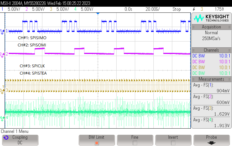
    The screenshot shows the signals between the two devices. Though both GPIO-19 on two boards are configured as SPISTEA with I/O. The SPISTEA signal still looks abnormal. I double-checked my connection on these two boars, I did not find any connection issue there. Will it work if I set another GPIO pin as the output to substitute the SPISTEA pin on the master device?

    SPI_GPIO_Init.txt
    //
    // InitSpiaGpio - This function initializes GPIO poins to function as SPI pins
    //
    void
    InitSpiaGpio()
    {
        EALLOW;
    
        //
        // Enable internal pull-up for the selected pins
        // Pull-ups can be enabled or disabled by the user.
        // This will enable the pullups for the specified pins.
        // Comment out other unwanted lines.
        //
        GpioCtrlRegs.GPAPUD.bit.GPIO16 = 0;   //Enable pull-up on GPIO16 (SPISIMOA)
        GpioCtrlRegs.GPAPUD.bit.GPIO17 = 0;   //Enable pull-up on GPIO17 (SPISOMIA)
        GpioCtrlRegs.GPAPUD.bit.GPIO18 = 0;   //Enable pull-up on GPIO18 (SPICLKA)
        GpioCtrlRegs.GPAPUD.bit.GPIO19 = 0;   //Enable pull-up on GPIO19 (SPISTEA)
    
        //GpioCtrlRegs.GPBPUD.bit.GPIO54 = 0; //Enable pull-up on GPIO54 (SPISIMOA)
        //GpioCtrlRegs.GPBPUD.bit.GPIO55 = 0; //Enable pull-up on GPIO55 (SPISOMIA)
        //GpioCtrlRegs.GPBPUD.bit.GPIO56 = 0; //Enable pull-up on GPIO56 (SPICLKA)
        //GpioCtrlRegs.GPBPUD.bit.GPIO57 = 0; //Enable pull-up on GPIO57 (SPISTEA)
    
        //
        // Set qualification for selected pins to asynch only
        // This will select asynch (no qualification) for the selected pins.
        // Comment out other unwanted lines.
        //
        GpioCtrlRegs.GPAQSEL2.bit.GPIO16 = 3; // Asynch input GPIO16 (SPISIMOA)
        GpioCtrlRegs.GPAQSEL2.bit.GPIO17 = 3; // Asynch input GPIO17 (SPISOMIA)
        GpioCtrlRegs.GPAQSEL2.bit.GPIO18 = 3; // Asynch input GPIO18 (SPICLKA)
        GpioCtrlRegs.GPAQSEL2.bit.GPIO19 = 3; // Asynch input GPIO19 (SPISTEA)
    
        //GpioCtrlRegs.GPBQSEL2.bit.GPIO54 = 3; // Asynch input GPIO16 (SPISIMOA)
        //GpioCtrlRegs.GPBQSEL2.bit.GPIO55 = 3; // Asynch input GPIO17 (SPISOMIA)
        //GpioCtrlRegs.GPBQSEL2.bit.GPIO56 = 3; // Asynch input GPIO18 (SPICLKA)
        //GpioCtrlRegs.GPBQSEL2.bit.GPIO57 = 3; // Asynch input GPIO19 (SPISTEA)
    
        //
        // Configure SPI-A pins using GPIO regs
        // This specifies which of the possible GPIO pins will be SPI
        // functional pins.
        // Comment out other unwanted lines.
        //
        GpioCtrlRegs.GPAMUX2.bit.GPIO16 = 1; // Configure GPIO16 as SPISIMOA
        GpioCtrlRegs.GPAMUX2.bit.GPIO17 = 1; // Configure GPIO17 as SPISOMIA
        GpioCtrlRegs.GPAMUX2.bit.GPIO18 = 1; // Configure GPIO18 as SPICLKA
        GpioCtrlRegs.GPAMUX2.bit.GPIO19 = 1; // Configure GPIO19 as SPISTEA
    
        //GpioCtrlRegs.GPBMUX2.bit.GPIO54 = 1; // Configure GPIO54 as SPISIMOA
        //GpioCtrlRegs.GPBMUX2.bit.GPIO55 = 1; // Configure GPIO55 as SPISOMIA
        //GpioCtrlRegs.GPBMUX2.bit.GPIO56 = 1; // Configure GPIO56 as SPICLKA
        //GpioCtrlRegs.GPBMUX2.bit.GPIO57 = 1; // Configure GPIO57 as SPISTEA
    
        EDIS;
    }
    

    Best regards

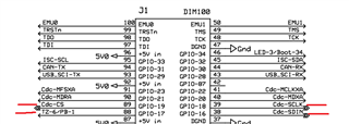
  • Can you please clarify which controlCARD revision and which docking station you are using? On this (www.ti.com/.../TMDSPREX28335) Explorer Kit the SPI pins you are using go to CODEC on the board. I don't see a way to disconnect GPIO19/SPISTE from the CODEC. Not sure if this is the board you are using though.

  • Hi Gus,

    Thank you for your help.

    I am using the evaluation kit of TMDSDOCK28335. The control card isTMDSCNCD28335 [R2.2]. The docking station is the one with the DIMM-100 socket in the following link:
    www.ti.com/.../sprufr5i.pdf

    If GPIO-19 is used on this docking station, can I use GPIO-57 as the SPISTEA? Meanwhile, the GPIO-57 is not layout on the docking board, it seems that I need to solder a jumper wire from the DIMM-100 pin.

    Best regards,

  • Thank so much for clarifying the boards you were using. This helps a lot. The GPIO19 should work, so not sure why you are not seeing it toggle. One thing I did notice is that you configure GPIO19 as SPISTEA in the pimux, but still use GPIO set and clear instructions. When configured as SPISTEA, the pin will be driven by the master directly, no need to use the GPIO set/clear functions.

    A couple of things you can try:

    • On the master side, configure GPIO19 as GPIO and try to toggle using set/clear functions. Note, on the slave side, you will need to use GPIO19 configured as SPISTEA.
    • If GPIO19 is not toggling, try temporarily disconnecting the GPIO19 pin between master/slave to see if the master can toggle this pin.
    • Lastly, try using any other GPIO pin as chip select on the master side. In this case, you want to configure the pin as GPIO and use set/clear instructions to toggle the pin. On the slave side, you will need to use GPIO19 configured as SPISTEA.
  • Hi Gus,

    Thank you for your advice on the SPISTEA pins. So far, I have made the SPI works with 16-word FIFO TX/RX buffers between two F28335 MCUs. The baud rate is set as 400 kbps and the data transfer at a frequency of 50Hz.
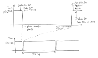
    The code is running in the infinite loop by polling the register bits of SpiaRegs.SPIFFRX.bit.RXFFST. Once its value reaches 16, the software will pop the RXFIFO. As for the TXFIFO, the master device pushes the data into it in the ADC interrupt before the communication starts. And the slave device pushes while the register SpiaRegs.SPIFFTX.bit.TXFFST is 0. Here there is a major delay in the data transmitted from the slave to the master.
    And here is the sequence in that I push/pop data into/from FIFO buffers.

    ---PICTURE---

    Therefore, the data transmitted from the master to the slave is less delayed. The data from the slave to the master has a delay of ~20ms. Do you have any suggestions that I can shorten this delay?

    Best regards,

  • Zhonghui,

    Good to know the issue was resolved. I'm curious to know what the resolution?

    Regarding your new question: the slave can only transmit data when the master generates a clock. Since your master is only transmitting data every 20ms (50Hz), it will take that long for data from the slave to reach the master in your current implementation. If you need it sooner, one thing you could do is have the master transmit an extra dummy word every 20ms. Therefore, in this dummy period, the slave can send data back to the master.