Other Parts Discussed in Thread: UNIFLASH, C2000WARE, SYSCONFIG, , TMS320F280039C
Hello,
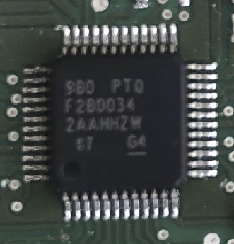
for some days I am struggling to make this F280034 run in standalone mode. I started off with the LAUNCHXL_F280039 board. The code runs there with no problem booting from flash. I tried to move to my custom board with F280034. I updated the liker file becuase in 0034 it starts from 0x88000 and in 0039 it starts from 0x80000:
/*
//###########################################################################
//
// FILE:	F280034_flash_lnk.cmd
//
// TITLE:	Linker Command File For F280034 Device
//
//###########################################################################
*/
MEMORY
{

   BOOT_RSVD		: origin = 0x00000002, length = 0x00000126

   RAMM0           	: origin = 0x00000128, length = 0x000002D8
   RAMM1            : origin = 0x00000400, length = 0x000003F8     /* on-chip RAM block M1 */
// RAMM1_RSVD       : origin = 0x000007F8, length = 0x00000008 /* Reserve and do not use for code as per the errata advisory "Memory: Prefetching Beyond Valid Memory" */


   RAMLS0           : origin = 0x00008000, length = 0x00000800
   RAMLS1           : origin = 0x00008800, length = 0x00000800
   RAMLS2           : origin = 0x00009000, length = 0x00000800
   RAMLS3           : origin = 0x00009800, length = 0x00000800
   RAMLS4           : origin = 0x0000A000, length = 0x00000800
   RAMLS5           : origin = 0x0000A800, length = 0x00000800
   RAMLS6           : origin = 0x0000B000, length = 0x00000800
   RAMLS7           : origin = 0x0000B800, length = 0x00000800

   /* Combining all the LS RAMs */
   //RAMLS            : origin = 0x00008000, length = 0x00004000

   RAMGS0           : origin = 0x0000C000, length = 0x00001000
   RAMGS1           : origin = 0x0000D000, length = 0x00001000
   RAMGS2           : origin = 0x0000E000, length = 0x00001000
   RAMGS3           : origin = 0x0000F000, length = 0x00000FF8
// RAMGS3_RSVD       : origin = 0x000FFF8, length = 0x00000008 /* Reserve and do not use for code as per the errata advisory "Memory: Prefetching Beyond Valid Memory" */

   BOOTROM          : origin = 0x003F8000, length = 0x00007FC0
   SECURE_ROM       : origin = 0x003F2000, length = 0x00006000

   RESET            : origin = 0x003FFFC0, length = 0x00000002
/*
#ifdef __TI_COMPILER_VERSION__
   #if __TI_COMPILER_VERSION__ >= 20012000
   #endif
#endif

 */
  BEGIN           	: origin = 0x00088000, length = 0x00000002
   /* Flash sectors */
   /* BANK 0 */
   FLASH_BANK0_SEC0  : origin = 0x088002, length = 0x000FFE
   FLASH_BANK0_SEC1  : origin = 0x089000, length = 0x001000
   FLASH_BANK0_SEC2  : origin = 0x08a000, length = 0x001000
   FLASH_BANK0_SEC3  : origin = 0x08b000, length = 0x001000
   FLASH_BANK0_SEC4  : origin = 0x08c000, length = 0x001000
   FLASH_BANK0_SEC5  : origin = 0x08d000, length = 0x001000
   FLASH_BANK0_SEC6  : origin = 0x08e000, length = 0x001000
   FLASH_BANK0_SEC7  : origin = 0x08f000, length = 0x000FF0
   FLASH_BANK0_SEC7_DO_NOT_USE : origin = 0x08FFF0, length = 0x000010  /* Reserve and do not use for code as per the errata advisory "Memory: Prefetching Beyond Valid Memory" */

   /* BANK 1 */
   FLASH_BANK1_SEC0  : origin = 0x090000, length = 0x001000
   FLASH_BANK1_SEC1  : origin = 0x091000, length = 0x001000
   FLASH_BANK1_SEC2  : origin = 0x092000, length = 0x001000
   FLASH_BANK1_SEC3  : origin = 0x093000, length = 0x001000
   FLASH_BANK1_SEC4  : origin = 0x094000, length = 0x001000
   FLASH_BANK1_SEC5  : origin = 0x095000, length = 0x001000
   FLASH_BANK1_SEC6  : origin = 0x096000, length = 0x001000
   FLASH_BANK1_SEC7  : origin = 0x097000, length = 0x000FF0
   FLASH_BANK1_SEC7_DO_NOT_USE : origin = 0x097FF0, length = 0x000010  /* Reserve and do not use for code as per the errata advisory "Memory: Prefetching Beyond Valid Memory" */
/*
#ifdef __TI_COMPILER_VERSION__
  #if __TI_COMPILER_VERSION__ >= 20012000
}  crc(_ccs_flash_checksum, algorithm=C28_CHECKSUM_16)
  #endif
#endif
*/
}


SECTIONS
{
   codestart        : > BEGIN, ALIGN(8)
   .text            : >> FLASH_BANK0_SEC2 | FLASH_BANK0_SEC3 | FLASH_BANK0_SEC4,   ALIGN(8)
   .cinit           : > FLASH_BANK0_SEC1,  ALIGN(8)
   .switch          : > FLASH_BANK0_SEC1,  ALIGN(8)
   .reset           : > RESET,                  TYPE = DSECT /* not used, */

   .stack           : > RAMM1

#if defined(__TI_EABI__)
   .init_array      : > FLASH_BANK0_SEC1,  ALIGN(8)
   .bss             : > RAMLS5
   .bss:output      : > RAMLS3
   .bss:cio         : > RAMLS0
   .data            : > RAMLS5
   .sysmem          : > RAMLS5
   .const           : > FLASH_BANK0_SEC4,  ALIGN(8)
#else
   .pinit           : > FLASH_BANK0_SEC1,  ALIGN(8)
   .ebss            : > RAMLS5
   .esysmem         : > RAMLS5
   .cio             : > RAMLS0
   .econst          : > FLASH_BANK0_SEC4,  ALIGN(8)
#endif

    ramgs0 : > RAMGS0
    ramgs1 : > RAMGS0

    /*  Allocate IQ math areas: */
   IQmath           : > FLASH_BANK0_SEC1, ALIGN(8)
   IQmathTables     : > FLASH_BANK0_SEC2, ALIGN(8)

   .TI.ramfunc      : LOAD = FLASH_BANK0_SEC1,
                      RUN = RAMLS0,
                      LOAD_START(RamfuncsLoadStart),
                      LOAD_SIZE(RamfuncsLoadSize),
                      LOAD_END(RamfuncsLoadEnd),
                      RUN_START(RamfuncsRunStart),
                      RUN_SIZE(RamfuncsRunSize),
                      RUN_END(RamfuncsRunEnd),
                      ALIGN(8)

   /* crc/checksum section configured as COPY section to avoid including in executable */
   .TI.memcrc          : type = COPY

}
/*
//###########################################################################
// End of file.
//###########################################################################
*/
What I did afterwards was to adjust the GEL file. The one provided with CCS was not adapted for the start address of 0x88000 and I could not flash with the X110 debugger. It was complaining that the address 0x80000 is not available or something similar. I replaced
    ...
    GEL_MapAddStr(0x00080000,0, 0x10000, "R|AS2",0);                     /*   FLASH BANK0 (128 KBytes)                                */
    ...
    GEL_MapAddStr(0x00080000,1, 0x10000, "R|AS2",0);                     /*   FLASH BANK0 (64 KBytes)                                */
    GEL_MapAddStr(0x00090000,1, 0x10000, "R|AS2",0);                     /*   FLASH BANK1 (64 KBytes)                                */
    GEL_MapAddStr(0x01080000,1, 0x2000, "R|AS2",0);                      /*   FLASH BANK0 ECC (16 KBytes)                             */
    GEL_MapAddStr(0x01082000,1, 0x2000, "R|AS2",0);                      /*   FLASH BANK0 ECC (16 KBytes)                             */
    ...
with this one:
    ...
    GEL_MapAddStr(0x00088000,0, 0x10000, "R|AS2",0);                     /*   FLASH BANK0 (128 KBytes)                                */
    ...
    GEL_MapAddStr(0x00088000,1, 0x8000, "R|AS2",0);                      /*   FLASH BANK0 (64 KBytes)                                */
    GEL_MapAddStr(0x00090000,1, 0x8000, "R|AS2",0);                      /*   FLASH BANK1 (64 KBytes)                                */
    GEL_MapAddStr(0x01081000,1, 0x1000, "R|AS2",0);                      /*   FLASH BANK0 ECC (16 KBytes)                             */
    GEL_MapAddStr(0x01082000,1, 0x1000, "R|AS2",0);                      /*   FLASH BANK0 ECC (16 KBytes)                             */
    ...
After flashing, the code runs properly with a debugger. In the "codestart" section I have
WD_DISABLE .set 1 ;set to 1 to disable WD, else set to 0
so watchdog should be disabled immediately after reaching my code. But when I disconnect the debugger and do a HW reset, then the microcontroller starts resetting. Both of the pins GPIO24 and GPIO32 are set to HIGH and I do not expect a HW issue, the board is already verified and the HW works as expected (still I tried with 2 boards just to be sure that there was no HW problem somewhere). So the MCU should boot from flash. But on XRS pin I can see periodic pulses for around 50us every 20ms as seen in the image below. This seems like a watchdog reset, but I cannot be completely sure. This pin is "open drain" on the other side so the component on the other side should not have any impact on the behaviour of this MCU.

I tried since then many different things. I have ticked "auto ECC generation" in the debugger settings and I can see in the ECC memory some data. So the ECC seems to be there.Then I found that the BootROM will probably jump to the entry address in flash if it is configured that way (as it is in my case). But since the probably default option 0 is address 0x80000 (check image below), then I thought that I have to write in the OTP that I want the entry point to be 0x88000.
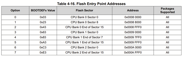
So I tried to write on address 0x78008 --> 0x5AFFFF20 so that it boots only dependent on GPIO32. And in 0x7800C --> 0x00000C23. First option is to boot from flash at address 0x88000, second is to flash from SPI.
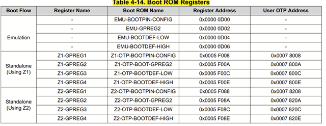
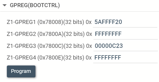
I am not able to write to the OTP. I tried adding this in the code, but I could not make it compile properly with the FAPI code. Then I tried adding it to the linker file, but it does not get flashed. I can see the data at this address in the "out" file (actually checking it in the s19 file that is generated by hex2000), but if I flash with XDS110 this image and then check with the "memory browser" I see only 0xFF at this addresses. Then I tried the same thing with Uniflash, again it did not succeed. Then I tried both in CCS and Uniflash to manually write these registers as seen below.
the error I get from both CCS and Uniflash is:
Since this was the first custom board I thought that maybe OTP was written unintentionally before and is already locked (even if it has the value 0xFF in all these registers). Then I took another custom board from the same type and without flashing any SW, just reading the memory to be sure that it is new, then directly writing these OTP registers, it failed agian in the same way.
I am running out of ideas. Does anybody have ideas what the problem could be? Do I need at all to flash the OTP of 0034 so that it jumps to 0x88000 or is this the default entry point on this MCU? Why do I see this reset on the XRS pin? What could this be? My assumption is that my code is not executed at all, it gets reset before reaching it.
thank you