This thread has been locked.

If you have a related question, please click the "Ask a related question" button in the top right corner. The newly created question will be automatically linked to this question.

TMS320F28384S: The DSP's SPI bus output waveform is not standard, the clock includes wide and narrow and the sampling edge aligns with the data edge

Part Number: TMS320F28384S

Hi team,

Here's an issue from the customer may need your help:

Use the syscfg tool configuration to generate the following SPI initialization code to access the SPI serial flash. When reading the device ID, send a 0x90 command to flash. The measurement waveform is shown in the following figure:

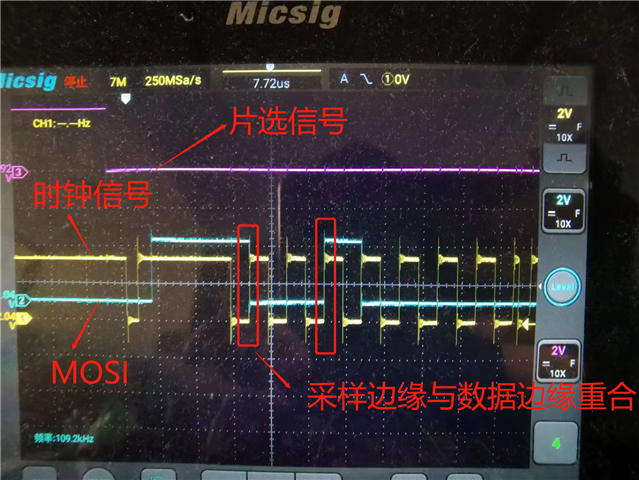
It was found that the waveform clock generated by the DSP chip is essentially aligned with the edges of the MOSI line, causing the device ID to not be read correctly.

So the customer would like to know are there any initialization configurations that can be used to optimize the waveform?
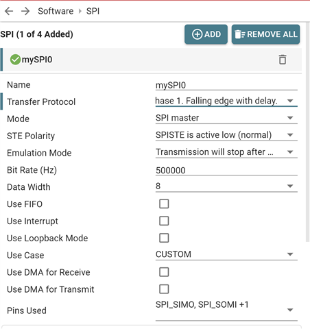
void mySPI0_init(){
SPI_disableModule(mySPI0_BASE);
SPI_setConfig(mySPI0_BASE, DEVICE_LSPCLK_FREQ, SPI_PROT_POL1PHA1,
SPI_MODE_MASTER, 500000, 8);
SPI_disableFIFO(mySPI0_BASE);
SPI_disableLoopback(mySPI0_BASE);
SPI_setEmulationMode(mySPI0_BASE, SPI_EMULATION_STOP_AFTER_TRANSMIT);
SPI_enableModule(mySPI0_BASE);
}

Could you help check this case? Thanks.

Best Regards,

Cherry

  • Cherry,

    SPI support four different SPICLK schemes. I see that you are using Falling edge with delay (CLKPOLARITY = 1, CLK_PHASE = 1). What clocking scheme does SPI serial FLASH expect? Check the SPI serial FLASH datasheet clocking scheme and compare against clocking scheme shown here.

    Regards,

    Manoj

  • Hi Manoj,

    Thanks for your support.

    The SPICLK scheme used by the customer is correct.

    Regardless of the clocking scheme, as the master side, the output clock should be at least stable,right (including period, frequency, etc.)? However, in the actual measured waveform, the clock is sometimes wide, sometimes narrow, and uneven. Is it a common behavior OR just anything wrong? 

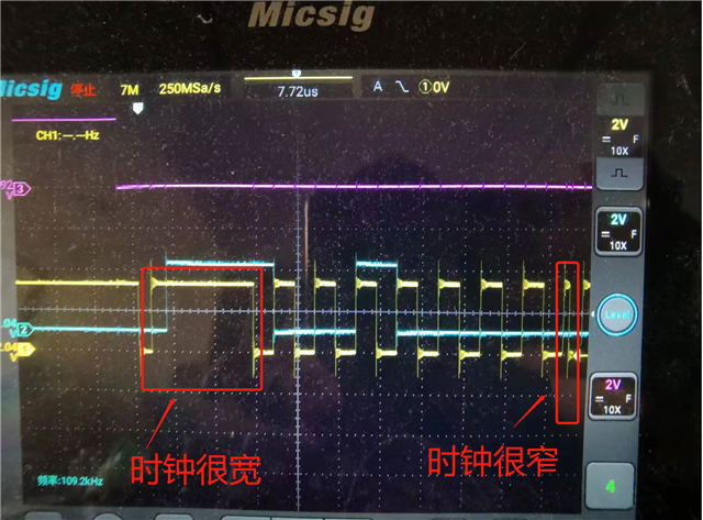
     (the red blocks represent the wide and narrow clock)

    Thanks and regards,

    Cherry

  • Cherry,

    Thanks for your support.

    The SPICLK scheme used by the customer is correct.

    I have seen many customer make mistake on the clocking scheme. It is really important to compare the clocking scheme (timing diagram) shown in SPI Flash datasheet with SPI clocking scheme mentioned in F280039 SPI TRM chapter. SPI clocking scheme mode (0/1/2/3) definitions mentioned in various datasheet are different and can be misleading. Can you send the SPI flash datasheet to confirm?

    Regardless of the clocking scheme, as the master side, the output clock should be at least stable,right (including period, frequency, etc.)? However, in the actual measured waveform, the clock is sometimes wide, sometimes narrow, and uneven. Is it a common behavior OR just anything wrong? 

    Clock frequency and duty cycle of SPI clock shouldn't change. Clearly something is wrong here.

    Do you see this problem is customer board (or) in launchpad? Can you check the waveform in launchpad to rule out any customer board issue?

    Regards,

    Manoj