This thread has been locked.

If you have a related question, please click the "Ask a related question" button in the top right corner. The newly created question will be automatically linked to this question.

TMS320F280039C: TMS320F280039C

Part Number: TMS320F280039C
Other Parts Discussed in Thread: TIDM-02010, SYSCONFIG

Hi,

Can you please help me in understanding how to configure the ADC module for a custom target board? I do not understand how the ADC is being configured in the following example:

// Three-shunt
#define MTR1_ADC_TRIGGER_SOC ADC_TRIGGER_EPWM1_SOCA // EPWM1_SOCA
#define MTR1_ADC_I_SAMPLEWINDOW 18
#define MTR1_ADC_V_SAMPLEWINDOW 26

#define MTR1_IU_ADC_BASE ADCC_BASE // ADCC-B12/C2*
#define MTR1_IV_ADC_BASE ADCB_BASE // ADCB-A11/B10*/C0
#define MTR1_IW_ADC_BASE ADCA_BASE // ADCA-A14*/B14/C4

#define MTR1_IU_ADCRES_BASE ADCCRESULT_BASE // ADCC-B12/C2*
#define MTR1_IV_ADCRES_BASE ADCBRESULT_BASE // ADCB-A11/B10*/C0
#define MTR1_IW_ADCRES_BASE ADCARESULT_BASE // ADCA-A14*/B14/C4


#define MTR1_IU_ADC_CH_NUM ADC_CH_ADCIN2 // ADCC-B12/C2*
#define MTR1_IV_ADC_CH_NUM ADC_CH_ADCIN10 // ADCB-A11/B10*/C0
#define MTR1_IW_ADC_CH_NUM ADC_CH_ADCIN14 // ADCA-A14*/B14/C4

#define MTR1_IU_ADC_SOC_NUM ADC_SOC_NUMBER1 // ADCC-B12/C2* -SOC1-PPB1
#define MTR1_IV_ADC_SOC_NUM ADC_SOC_NUMBER1 // ADCB-A11/B10*/C0 -SOC1-PPB1
#define MTR1_IW_ADC_SOC_NUM ADC_SOC_NUMBER1 // ADCA-A14*/B14/C4 -SOC1-PPB1

#define MTR1_IU_ADC_PPB_NUM ADC_PPB_NUMBER1 // ADCC-B12/C2* -SOC1-PPB1
#define MTR1_IV_ADC_PPB_NUM ADC_PPB_NUMBER1 // ADCB-A11/B10*/C0 -SOC1-PPB1
#define MTR1_IW_ADC_PPB_NUM ADC_PPB_NUMBER1 // ADCA-A14*/B14/C4 -SOC1-PPB1

Please let me know if you have any questions or would like additional information.

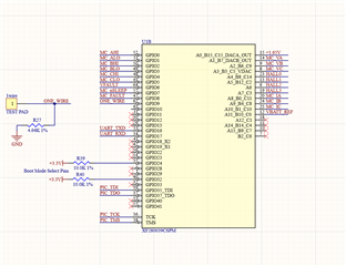
I can provide schematic reference for the setup of my target device with the F280039C if that helps.

Thank you,
William

  • Hi William,

    What example project is this? The Universal Motor Lab or TIDM-02010?

    For a custom board you should only need to make changes to the defines in hal.h file. These defines are used in HAL_setupADCs() function found in hal.c file for configuring the ADC module.

    In the code comments the asterisks is used to mark what ADC channel is being configured by default. For example, ADC-C channel 2 is represented by the below (C2*). This would match up with the respective pin on the F28003x device / schematic being used for sensing U-phase current. Hopefully this helps with part of your questions.

    #define MTR1_IU_ADC_BASE ADCC_BASE // ADCC-B12/C2*

    Best,

    Kevin

  • Hi Kevin,

    An overview of the present issue is configuring the ADC channels on our custom target board.  I started with the “universal_motorcontrol_lab_f28003x” CCS project.  I made a change to use the internal oscillator because our target board does not have a crystal oscillator.  I then changed the hal.c and hal.h files to NOT setup GPIO_35 (TDI) and GPIO_37 (TDO) as GPIO pins because it was preventing me from being able to connect and emulate via JTAG.  

    I then changed the following source code in the hal.h file from this:

    // !MOTOR1_DCLINKSS, Three-shunt

    // Three-shunt

    #define MTR1_ADC_TRIGGER_SOC         ADC_TRIGGER_EPWM1_SOCA  // EPWM1_SOCA

    #define MTR1_ADC_I_SAMPLEWINDOW     18

    #define MTR1_ADC_V_SAMPLEWINDOW     26


    #define MTR1_IU_ADC_BASE        ADCC_BASE               // ADCC-B12/C2*

    #define MTR1_IV_ADC_BASE        ADCB_BASE               // ADCB-A11/B10*/C0

    #define MTR1_IW_ADC_BASE        ADCA_BASE               // ADCA-A14*/B14/C4


    #define MTR1_IU_ADCRES_BASE     ADCCRESULT_BASE         // ADCC-B12/C2*

    #define MTR1_IV_ADCRES_BASE     ADCBRESULT_BASE         // ADCB-A11/B10*/C0

    #define MTR1_IW_ADCRES_BASE     ADCARESULT_BASE         // ADCA-A14*/B14/C4


    #define MTR1_IU_ADC_CH_NUM      ADC_CH_ADCIN2           // ADCC-B12/C2*

    #define MTR1_IV_ADC_CH_NUM      ADC_CH_ADCIN10          // ADCB-A11/B10*/C0

    #define MTR1_IW_ADC_CH_NUM      ADC_CH_ADCIN14          // ADCA-A14*/B14/C4


    #define MTR1_IU_ADC_SOC_NUM     ADC_SOC_NUMBER1         // ADCC-B12/C2*     -SOC1-PPB1

    #define MTR1_IV_ADC_SOC_NUM     ADC_SOC_NUMBER1         // ADCB-A11/B10*/C0 -SOC1-PPB1

    #define MTR1_IW_ADC_SOC_NUM     ADC_SOC_NUMBER1         // ADCA-A14*/B14/C4 -SOC1-PPB1


    #define MTR1_IU_ADC_PPB_NUM     ADC_PPB_NUMBER1         // ADCC-B12/C2*     -SOC1-PPB1

    #define MTR1_IV_ADC_PPB_NUM     ADC_PPB_NUMBER1         // ADCB-A11/B10*/C0 -SOC1-PPB1

    #define MTR1_IW_ADC_PPB_NUM     ADC_PPB_NUMBER1         // ADCA-A14*/B14/C4 -SOC1-PPB1


    // CMPSS

    #define MTR1_CMPSS_U_BASE       CMPSS3_BASE

    #define MTR1_CMPSS_V_BASE       CMPSS1_BASE

    #define MTR1_CMPSS_W_BASE       CMPSS3_BASE


    #define MTR1_XBAROUTPUT         XBAR_OUTPUT7


    #define MTR1_IU_CMPHP_SEL       ASYSCTL_CMPHPMUX_SELECT_3    // CMPSS3-B12/C2*

    #define MTR1_IU_CMPLP_SEL       ASYSCTL_CMPLPMUX_SELECT_3    // CMPSS3-B12/C2*, N/A


    #define MTR1_IV_CMPHP_SEL       ASYSCTL_CMPHPMUX_SELECT_1    // CMPSS1-A11/B10*/C0

    #define MTR1_IV_CMPLP_SEL       ASYSCTL_CMPLPMUX_SELECT_1    // CMPSS1-A11/B10*/C0


    #define MTR1_IW_CMPHP_SEL       ASYSCTL_CMPHPMUX_SELECT_3    // CMPSS3-A14*/B14/C4, N/A

    #define MTR1_IW_CMPLP_SEL       ASYSCTL_CMPLPMUX_SELECT_3    // CMPSS3-A14*/B14/C4


    #define MTR1_IU_CMPHP_MUX       1                            // CMPSS3-B12/C2*

    #define MTR1_IU_CMPLP_MUX       1                            // CMPSS3-B12/C2*


    #define MTR1_IV_CMPHP_MUX       1                            // CMPSS1-A11/B10*/C0

    #define MTR1_IV_CMPLP_MUX       1                            // CMPSS1-A11/B10*/C0


    #define MTR1_IW_CMPHP_MUX       4                            // CMPSS3-A14*/B14/C4

    #define MTR1_IW_CMPLP_MUX       4                            // CMPSS3-A14*/B14/C4


    #define MTR1_IU_XBAR_EPWM_MUX   XBAR_EPWM_MUX04_CMPSS3_CTRIPH       // CMPSS3-HP

    #define MTR1_IV_XBAR_EPWM_MUX   XBAR_EPWM_MUX00_CMPSS1_CTRIPH_OR_L  // CMPSS1-HP&LP

    #define MTR1_IW_XBAR_EPWM_MUX   XBAR_EPWM_MUX05_CMPSS3_CTRIPL       // CMPSS3-LP


    #define MTR1_IU_XBAR_MUX        XBAR_MUX04          // CMPSS3-HP

    #define MTR1_IV_XBAR_MUX        XBAR_MUX00          // CMPSS1-HP&LP

    #define MTR1_IW_XBAR_MUX        XBAR_MUX05          // CMPSS3-LP


    #define MTR1_IU_XBAR_OUT_MUX    XBAR_OUT_MUX04_CMPSS3_CTRIPOUTH       // CMPSS3-HP, Not used

    #define MTR1_IV_XBAR_OUT_MUX    XBAR_OUT_MUX00_CMPSS1_CTRIPOUTH_OR_L  // CMPSS1-HP&LP, Not used

    #define MTR1_IW_XBAR_OUT_MUX    XBAR_OUT_MUX05_CMPSS3_CTRIPOUTL       // CMPSS3-LP, Not used

    #endif    // !MOTOR1_DCLINKSS, Three-shunt


    // ADC - Voltage, Phase and dc-bus

    #define MTR1_VU_ADC_BASE        ADCA_BASE               // ADCA-A6*

    #define MTR1_VV_ADC_BASE        ADCB_BASE               // ADCB-A2/B6*/C9

    #define MTR1_VW_ADC_BASE        ADCC_BASE               // ADCC-A3/B9/C7*

    #define MTR1_VDC_ADC_BASE       ADCC_BASE               // ADCC-B2/C6*

    #define MTR1_POT_ADC_BASE       ADCB_BASE               // ADCB-B3*


    #define MTR1_VU_ADCRES_BASE     ADCARESULT_BASE         // ADCA-A6*

    #define MTR1_VV_ADCRES_BASE     ADCBRESULT_BASE         // ADCB-A2/B6*/C9

    #define MTR1_VW_ADCRES_BASE     ADCCRESULT_BASE         // ADCC-A3/B9/C7*

    #define MTR1_VDC_ADCRES_BASE    ADCCRESULT_BASE         // ADCC-B2/C6*

    #define MTR1_POT_ADCRES_BASE    ADCBRESULT_BASE         // ADCB-B3*


    #define MTR1_VU_ADC_CH_NUM      ADC_CH_ADCIN6           // ADCA-A6*

    #define MTR1_VV_ADC_CH_NUM      ADC_CH_ADCIN6           // ADCB-A2/B6*/C9

    #define MTR1_VW_ADC_CH_NUM      ADC_CH_ADCIN7           // ADCC-A3/B9/C7*

    #define MTR1_VDC_ADC_CH_NUM     ADC_CH_ADCIN6           // ADCC-B2/C6*

    #define MTR1_POT_ADC_CH_NUM     ADC_CH_ADCIN3           // ADCB-B3*


    #define MTR1_VU_ADC_SOC_NUM     ADC_SOC_NUMBER2         // ADCA-A6*         -SOC2

    #define MTR1_VV_ADC_SOC_NUM     ADC_SOC_NUMBER2         // ADCB-A2/B6*/C9   -SOC2

    #define MTR1_VW_ADC_SOC_NUM     ADC_SOC_NUMBER2         // ADCC-A3/B9/C7*   -SOC2

    #define MTR1_VDC_ADC_SOC_NUM    ADC_SOC_NUMBER3         // ADCC-B2/C6*      -SOC3

    #define MTR1_POT_ADC_SOC_NUM    ADC_SOC_NUMBER3         // ADCB-B3*         -SOC3


    // interrupt

    #define MTR1_PWM_INT_BASE       MTR1_PWM_U_BASE         // EPWM1


    #define MTR1_ADC_INT_BASE       ADCC_BASE               // ADCC-C6  -SOC3

    #define MTR1_ADC_INT_NUM        ADC_INT_NUMBER1         // ADCC_INT1-SOC3

    #define MTR1_ADC_INT_SOC        ADC_SOC_NUMBER3         // ADCC_INT1-SOC3


    #define MTR1_PIE_INT_NUM        INT_ADCC1               // ADCC_INT1-SOC3

    #define MTR1_INT_ACK_GROUP      INTERRUPT_ACK_GROUP1    // ADCC_INT1-CPU_INT1


    //! \brief Defines the PWM deadband falling edge delay count (system clocks)

    #define MTR1_PWM_DBFED_CNT      5           // 50ns


    //! \brief Defines the PWM deadband rising edge delay count (system clocks)

    #define MTR1_PWM_DBRED_CNT      5           // 50ns


    // end of BSXL8323RH_REVB


    AND changed it to this to attempt to accommodate my custom target board which has the F280039CSPM:

    // !MOTOR1_DCLINKSS, Three-shunt

    // Three-shunt

    #define MTR1_ADC_TRIGGER_SOC         ADC_TRIGGER_EPWM1_SOCA  // EPWM1_SOCA

    #define MTR1_ADC_I_SAMPLEWINDOW     18

    #define MTR1_ADC_V_SAMPLEWINDOW     26


    #define MTR1_IU_ADC_BASE        ADCC_BASE               // ADCC-B12/C2*

    #define MTR1_IV_ADC_BASE        ADCB_BASE               // ADCB-A11/B10*/C0

    #define MTR1_IW_ADC_BASE        ADCA_BASE               // ADCA-A14*/B14/C4


    #define MTR1_IU_ADCRES_BASE     ADCCRESULT_BASE         // ADCC-B12/C2*

    #define MTR1_IV_ADCRES_BASE     ADCBRESULT_BASE         // ADCB-A11/B10*/C0

    #define MTR1_IW_ADCRES_BASE     ADCARESULT_BASE         // ADCA-A14*/B14/C4


    // WILLIAM

    #define MTR1_IU_ADC_CH_NUM      ADC_CH_ADCIN11           // ADCC-B12/C2*

    #define MTR1_IV_ADC_CH_NUM      ADC_CH_ADCIN4          // ADCB-A11/B10*/C0

    #define MTR1_IW_ADC_CH_NUM      ADC_CH_ADCIN10          // ADCA-A14*/B14/C4

    //#define MTR1_IU_ADC_CH_NUM      ADC_CH_ADCIN2           // ADCC-B12/C2*

    //#define MTR1_IV_ADC_CH_NUM      ADC_CH_ADCIN10          // ADCB-A11/B10*/C0

    //#define MTR1_IW_ADC_CH_NUM      ADC_CH_ADCIN14          // ADCA-A14*/B14/C4


    #define MTR1_IU_ADC_SOC_NUM     ADC_SOC_NUMBER1         // ADCC-B12/C2*     -SOC1-PPB1

    #define MTR1_IV_ADC_SOC_NUM     ADC_SOC_NUMBER1         // ADCB-A11/B10*/C0 -SOC1-PPB1

    #define MTR1_IW_ADC_SOC_NUM     ADC_SOC_NUMBER1         // ADCA-A14*/B14/C4 -SOC1-PPB1


    #define MTR1_IU_ADC_PPB_NUM     ADC_PPB_NUMBER1         // ADCC-B12/C2*     -SOC1-PPB1

    #define MTR1_IV_ADC_PPB_NUM     ADC_PPB_NUMBER1         // ADCB-A11/B10*/C0 -SOC1-PPB1

    #define MTR1_IW_ADC_PPB_NUM     ADC_PPB_NUMBER1         // ADCA-A14*/B14/C4 -SOC1-PPB1


    // CMPSS

    //#define MTR1_CMPSS_U_BASE       CMPSS3_BASE

    //#define MTR1_CMPSS_V_BASE       CMPSS1_BASE

    //#define MTR1_CMPSS_W_BASE       CMPSS3_BASE


    //#define MTR1_XBAROUTPUT         XBAR_OUTPUT7


    //#define MTR1_IU_CMPHP_SEL       ASYSCTL_CMPHPMUX_SELECT_3    // CMPSS3-B12/C2*

    //#define MTR1_IU_CMPLP_SEL       ASYSCTL_CMPLPMUX_SELECT_3    // CMPSS3-B12/C2*, N/A


    //#define MTR1_IV_CMPHP_SEL       ASYSCTL_CMPHPMUX_SELECT_1    // CMPSS1-A11/B10*/C0

    //#define MTR1_IV_CMPLP_SEL       ASYSCTL_CMPLPMUX_SELECT_1    // CMPSS1-A11/B10*/C0


    //#define MTR1_IW_CMPHP_SEL       ASYSCTL_CMPHPMUX_SELECT_3    // CMPSS3-A14*/B14/C4, N/A

    //#define MTR1_IW_CMPLP_SEL       ASYSCTL_CMPLPMUX_SELECT_3    // CMPSS3-A14*/B14/C4


    //#define MTR1_IU_CMPHP_MUX       1                            // CMPSS3-B12/C2*

    //#define MTR1_IU_CMPLP_MUX       1                            // CMPSS3-B12/C2*


    //#define MTR1_IV_CMPHP_MUX       1                            // CMPSS1-A11/B10*/C0

    //#define MTR1_IV_CMPLP_MUX       1                            // CMPSS1-A11/B10*/C0


    //#define MTR1_IW_CMPHP_MUX       4                            // CMPSS3-A14*/B14/C4

    //#define MTR1_IW_CMPLP_MUX       4                            // CMPSS3-A14*/B14/C4


    #define MTR1_IU_XBAR_EPWM_MUX   XBAR_EPWM_MUX04_CMPSS3_CTRIPH       // CMPSS3-HP

    #define MTR1_IV_XBAR_EPWM_MUX   XBAR_EPWM_MUX00_CMPSS1_CTRIPH_OR_L  // CMPSS1-HP&LP

    #define MTR1_IW_XBAR_EPWM_MUX   XBAR_EPWM_MUX05_CMPSS3_CTRIPL       // CMPSS3-LP


    #define MTR1_IU_XBAR_MUX        XBAR_MUX04          // CMPSS3-HP

    #define MTR1_IV_XBAR_MUX        XBAR_MUX00          // CMPSS1-HP&LP

    #define MTR1_IW_XBAR_MUX        XBAR_MUX05          // CMPSS3-LP


    //#define MTR1_IU_XBAR_OUT_MUX    XBAR_OUT_MUX04_CMPSS3_CTRIPOUTH       // CMPSS3-HP, Not used

    //#define MTR1_IV_XBAR_OUT_MUX    XBAR_OUT_MUX00_CMPSS1_CTRIPOUTH_OR_L  // CMPSS1-HP&LP, Not used

    //#define MTR1_IW_XBAR_OUT_MUX    XBAR_OUT_MUX05_CMPSS3_CTRIPOUTL       // CMPSS3-LP, Not used

    #endif    // !MOTOR1_DCLINKSS, Three-shunt


    // ADC - Voltage, Phase and dc-bus

    #define MTR1_VU_ADC_BASE        ADCA_BASE               // ADCA-A6*

    #define MTR1_VV_ADC_BASE        ADCB_BASE               // ADCB-A2/B6*/C9

    #define MTR1_VW_ADC_BASE        ADCC_BASE               // ADCC-A3/B9/C7*

    #define MTR1_VDC_ADC_BASE       ADCC_BASE               // ADCC-B2/C6*

    #define MTR1_POT_ADC_BASE       ADCB_BASE               // ADCB-B3*


    #define MTR1_VU_ADCRES_BASE     ADCARESULT_BASE         // ADCA-A6*

    #define MTR1_VV_ADCRES_BASE     ADCBRESULT_BASE         // ADCB-A2/B6*/C9

    #define MTR1_VW_ADCRES_BASE     ADCCRESULT_BASE         // ADCC-A3/B9/C7*

    #define MTR1_VDC_ADCRES_BASE    ADCCRESULT_BASE         // ADCC-B2/C6*

    #define MTR1_POT_ADCRES_BASE    ADCBRESULT_BASE         // ADCB-B3*


    //#define MTR1_VU_ADC_CH_NUM      ADC_CH_ADCIN6           // ADCA-A6*

    //#define MTR1_VV_ADC_CH_NUM      ADC_CH_ADCIN6           // ADCB-A2/B6*/C9

    //#define MTR1_VW_ADC_CH_NUM      ADC_CH_ADCIN7           // ADCC-A3/B9/C7*

    //#define MTR1_VDC_ADC_CH_NUM     ADC_CH_ADCIN6           // ADCC-B2/C6*

    //#define MTR1_POT_ADC_CH_NUM     ADC_CH_ADCIN3           // ADCB-B3*

    #define MTR1_VU_ADC_CH_NUM      ADC_CH_ADCIN1           // ADCA-A6*

    #define MTR1_VV_ADC_CH_NUM      ADC_CH_ADCIN6           // ADCB-A2/B6*/C9

    #define MTR1_VW_ADC_CH_NUM      ADC_CH_ADCIN5           // ADCC-A3/B9/C7*

    #define MTR1_VDC_ADC_CH_NUM     ADC_CH_ADCIN0           // ADCC-B2/C6*

    #define MTR1_POT_ADC_CH_NUM     ADC_CH_ADCIN8           // ADCB-B3*


    #define MTR1_VU_ADC_SOC_NUM     ADC_SOC_NUMBER2         // ADCA-A6*         -SOC2

    #define MTR1_VV_ADC_SOC_NUM     ADC_SOC_NUMBER2         // ADCB-A2/B6*/C9   -SOC2

    #define MTR1_VW_ADC_SOC_NUM     ADC_SOC_NUMBER2         // ADCC-A3/B9/C7*   -SOC2

    #define MTR1_VDC_ADC_SOC_NUM    ADC_SOC_NUMBER3         // ADCC-B2/C6*      -SOC3

    #define MTR1_POT_ADC_SOC_NUM    ADC_SOC_NUMBER3         // ADCB-B3*         -SOC3


    // interrupt

    #define MTR1_PWM_INT_BASE       MTR1_PWM_U_BASE         // EPWM1


    #define MTR1_ADC_INT_BASE       ADCC_BASE               // ADCC-C6  -SOC3

    #define MTR1_ADC_INT_NUM        ADC_INT_NUMBER1         // ADCC_INT1-SOC3

    #define MTR1_ADC_INT_SOC        ADC_SOC_NUMBER3         // ADCC_INT1-SOC3


    #define MTR1_PIE_INT_NUM        INT_ADCC1               // ADCC_INT1-SOC3

    #define MTR1_INT_ACK_GROUP      INTERRUPT_ACK_GROUP1    // ADCC_INT1-CPU_INT1


    //! \brief Defines the PWM deadband falling edge delay count (system clocks)

    #define MTR1_PWM_DBFED_CNT      5           // 50ns


    //! \brief Defines the PWM deadband rising edge delay count (system clocks)

    #define MTR1_PWM_DBRED_CNT      5           // 50ns


    // end of BSXL8323RH_REVB


    My target board has the following schematic:

    I need all A/D signals to be properly converted.  But right now my main focus is to get the motor phase current, phase voltage, and battery voltage converted properly.  I checked the hardware and the current feedback circuits measure 1.65 vdc with no current as expected, the battery voltage measures 2.5 vdc with the nominal bus voltage of 9.9 vdc, and the phase voltage feedbacks measure 0 vdc with no motor bemf, all as expected.  However, the A/D values in CCS in debug mode are bouncing around all over the place.  So, I assume I am missing something or not configuring something properly, which I have not figured out yet.  Below you can observe two screenshots of the adcData and it is bouncing around a lot. 

    I have read through the Motor Control SDK Universal Project and Lab, as well as, the datasheet and the Technical Reference Manual for the F280039C without finding a solution.   

    Please let me know if you have any additional questions. I look forward to learning what I am missing with your help.


    Thank you,

    William

  • Also, I am compiling the project with the Flash_lib_DRV8323RH_3SC configuration.

  • Hi William,

    Which build level are you testing with? You should run them in sequential order and verify things are working properly before moving onto the next level.

    Below you can observe two screenshots of the adcData and it is bouncing around a lot.

    Are you running your motor in this example? It can help to plot the parameters using the CCS graph tool or outputting them on the device's DAC. That way you can see if the shape of the phase current / voltage are correct or not.

    Best,

    Kevin

  • Hi Kevin,

    Build Level 1 and no motor connected.

    Regards,

    William

  • Hi William,

    Build Level 1 and no motor connected.

    OK, I think I better understand the issue now, but please help me confirm.

    I checked the hardware and the current feedback circuits measure 1.65 vdc with no current as expected, the battery voltage measures 2.5 vdc with the nominal bus voltage of 9.9 vdc, and the phase voltage feedbacks measure 0 vdc with no motor bemf, all as expected. 

    The above is based on checking the sensing signals with a multi-meter / oscilloscope? This is not C2000 ADC readings.

    However, the A/D values in CCS in debug mode are bouncing around all over the place.  So, I assume I am missing something or not configuring something properly, which I have not figured out yet.  Below you can observe two screenshots of the adcData and it is bouncing around a lot. 

    Are PWMs toggling at this point? I wonder if there is some coupling from the PWMs onto the ADC signals if so.

    Can you plot the sensed current & voltage values using CCS graph tool to see if there is some shape to them? Also, have you verified the current and voltage offset values are correct (per User's Guide).

    Best,

    Kevin

  • Hi Kevin,

    Correct, the above that you mentioned was based on checking the signals with an oscilloscope and was not the C2000 ADC readings. The ADC readings are sporadic as I showed in the screenshots.

    The ADC readings were monitored with the PWMs ON and OFF and were bouncing/sporadic in both cases.  

    I did not plot the current and voltage values using the CCS graph tool because with no motor running and therefore no voltage and no current with no PWM the ADC values should be reading the DC values I measure on the scope (as mentioned above).  The current and voltage offset values are also incorrect.  The ADC module is no converting properly for some reason.  That is the main issue I am having. I think it has something to do with the setup and configuration in the firmware but I am not sure what.

    Regards,

    William

  • Hi Kevin,

    Shown below is a scope waveform of the VBATT_REF pin of my schematic, which correlates to pin-12 of the F280039CSPM (A11_B10_C0*).

    As you can observe, there is no oscillation, and the signal is a steady 2.56 V DC, which would correlate to an ADC Value of 3178 UDEC. 

    Please let me know what else you think may be causing this issue.  I noticed in the SYSCONFIG file it says this ADC "C0" pin is something other than pin-12, could it be an error due to the different F280039C package (we are using the 64-pin package)?

    Regards,

    William

  • Hi William,

    Thanks for providing the oscilloscope waveform. There is no significant noise on the signal from it and from the ADC readings you showed it would have to be some drastic noise on the signal (i.e. seeing 2000-4000 swings in ADC readings).

    I noticed in the SYSCONFIG file it says this ADC "C0" pin is something other than pin-12, could it be an error due to the different F280039C package (we are using the 64-pin package)?

    This should not have any impact. Sysconfig will configure the specific ADC channel regardless of package pin.

    Let's continue the discussion and debug off-forum. Once we find a resolution it can be posted on this E2E for closure.

    Best,

    Kevin

  • Primary issue was identified, VREFHI pin was missing an external capacitor to ground / VREFLO. After the capacitor was added ADC sampling is working properly.

    Best,

    Kevin