


Part Number: TMS320F28379D
Hi team,
Here's an issue from the customer may need your help:
Project: Flying capacitor type three-level buck circuit.
The customer uses the 28379D launchpad to do a single voltage closed loop (flying capacitor voltage balance is not yet controlled) where the output voltage starts to drop after the input reaches above 20V. The assumptions are as follows:
1) The isolated amplifier + normal op amp conditioning circuit is selected for sampling and has been tested with a stable DC voltage without problems.
2) With a custom board, the same voltage is output at different duty cycles in open loop (e.g. 20V output 8V, 30V output 8V), the output voltage of the sampling circuit is higher with a multimeter at high voltage input, and the same data is obtained when checking the monolithic unit at the computer side.
3) The problem persists after replacing the power plate to plate wiring with shielding and trying to reduce interference.
4) The following are the waveforms of the output voltage at an input of approximately 30V:

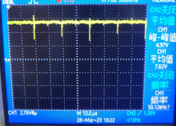
Based on points 3) and 4), the customer assumes that the output voltage effective value is higher due to the shut-off spike of the output voltage at high voltage, so the sampling value of the monolithic machine is higher and the duty cycle of the control switch is reduced. So the following changes were made:
The switching frequency is 50 kHz. Sampling Frequency = Switching Frequency, the problem persists after trying to avoid spikes by modifying the sampling point to 3/4 of the switching period.
And please see the code below:
void ConfigureADC(void)
{
    EALLOW;
    AdcaRegs.ADCCTL2.bit.PRESCALE = 0; //ADC clock divider
    AdcSetMode(ADC_ADCA, ADC_RESOLUTION_12BIT, ADC_SIGNALMODE_SINGLE);//Sets the ADC operating mode: 12-bit single input signal
    AdcaRegs.ADCCTL1.bit.INTPULSEPOS = 1;//An interrupt pulse is generated after the conversion is complete
    AdcaRegs.ADCCTL1.bit.ADCPWDNZ = 1;//Turn on all analogue circuits
    DELAY_US(1000);

    AdcbRegs.ADCCTL2.bit.PRESCALE = 0; //ADC clock divider
    AdcSetMode(ADC_ADCB, ADC_RESOLUTION_12BIT, ADC_SIGNALMODE_SINGLE);//Sets the ADC operating mode: 12-bit single input signal
    AdcbRegs.ADCCTL1.bit.INTPULSEPOS = 1;//An interrupt pulse is generated after the conversion is complete
    AdcbRegs.ADCCTL1.bit.ADCPWDNZ = 1;//Turn on all analogue circuits
    DELAY_US(1000);

    AdccRegs.ADCCTL2.bit.PRESCALE = 0; //ADC clock divider
    AdcSetMode(ADC_ADCC, ADC_RESOLUTION_12BIT, ADC_SIGNALMODE_SINGLE);//Sets the ADC operating mode: 12-bit single input signal
    AdccRegs.ADCCTL1.bit.INTPULSEPOS = 1;//An interrupt pulse is generated after the conversion is complete
    AdccRegs.ADCCTL1.bit.ADCPWDNZ = 1;//Turn on all analogue circuits
    DELAY_US(1000);
    EDIS;
}

void ConfigureEPWM(void)
{
    EALLOW;
    // Assumes ePWM clock is already enabled
    EPwm1Regs.ETSEL.bit.SOCAEN    = 0;    // Disables the EWPWMxSOCA pulses
    EPwm1Regs.ETSEL.bit.SOCASEL   = 4;   // Up counting
    EPwm1Regs.ETPS.bit.SOCAPRD = 1;       // Pulse is generated on Event 1
    //The following needs to be set for single sampling and is configured again in this procedure in the PWM configuration function
    EPwm1Regs.CMPA.bit.CMPA = 750;     // Set compare A value to 2048 counts
    EPwm1Regs.TBPRD = 999;             // Set period to 4096 counts
    EPwm1Regs.TBCTL.bit.CTRMODE = 3;      // freeze counter
    EDIS;
}

void SetupADCEpwm(void)
{
    Uint16 acqps = 25;

    EALLOW;
    AdcaRegs.ADCSOC0CTL.bit.CHSEL = 0;  //SOC0 convert to A0
    AdcaRegs.ADCSOC0CTL.bit.ACQPS = acqps; //Sets the sampling window time
    AdcaRegs.ADCSOC0CTL.bit.TRIGSEL = 5; //trigger signal - ePWM1, ADCSOCA
    AdcaRegs.ADCINTSEL1N2.bit.INT1SEL = 0; //EOC0 is trigger for ADCINT1
    AdcaRegs.ADCINTSEL1N2.bit.INT1E = 1;   //Enable interrupt flag bit
    AdcaRegs.ADCINTFLGCLR.bit.ADCINT1 = 1; //make sure INT1 flag is cleared

    AdcbRegs.ADCSOC0CTL.bit.CHSEL = 2;  //SOC0 convert to B2
    AdcbRegs.ADCSOC0CTL.bit.ACQPS = acqps; //Sets the sampling window time
    AdcbRegs.ADCSOC0CTL.bit.TRIGSEL = 5; //trigger signal - ePWM1, ADCSOCA
    AdcbRegs.ADCINTSEL1N2.bit.INT1SEL = 0; //EOC0 is trigger for ADCINT1
    AdcbRegs.ADCINTSEL1N2.bit.INT1E = 1;   //Enable interrupt flag bit
    AdcbRegs.ADCINTFLGCLR.bit.ADCINT1 = 1; //make sure INT1 flag is cleared

    AdccRegs.ADCSOC0CTL.bit.CHSEL = 2;  //SOC0 convert to C2
    AdccRegs.ADCSOC0CTL.bit.ACQPS = acqps; //Sets the sampling window time
    AdccRegs.ADCSOC0CTL.bit.TRIGSEL = 5; //trigger signal - ePWM1, ADCSOCA
    AdccRegs.ADCINTSEL1N2.bit.INT1SEL = 0; //EOC0 is trigger for ADCINT1
    AdccRegs.ADCINTSEL1N2.bit.INT1E = 1;   //Enable interrupt flag bit
    AdccRegs.ADCINTFLGCLR.bit.ADCINT1 = 1; //make sure INT1 flag is cleared
    EDIS;
}
Customers want to try to reduce the shutdown spike by adding RC snubber to see if the problem can improve, but MOS package and board layout do not allow it.
Could you help check this case? Thanks.
Best Regards,
Cherry
