This thread has been locked.

If you have a related question, please click the "Ask a related question" button in the top right corner. The newly created question will be automatically linked to this question.

LAUNCHXL-F280049C: SR Mode 2 misoperation at PSFB control

Part Number: LAUNCHXL-F280049C
Other Parts Discussed in Thread: PMP23126, TIDM-02009, C2000WARE,

Hi,

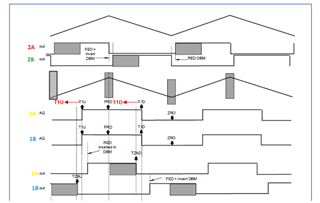
Nowadays, I'm trying to test my PCMC software in SR mode 2. It is event based software that is explained in PMP23126 and TIDM-02009. I explained as below.

I used demoboard of F280049C to test the software. I'm trying to test inner loop (PCMC) with SR mode 2 and I designed my software using reference software.

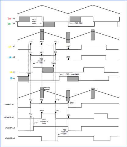
Test case on demoboard F280049C is as below.  I just implemented inner CMPSS configuration and trying test whether it is working or not. It is event based CMPSS software that is explained for both PMP23126 and TIDM-02009.

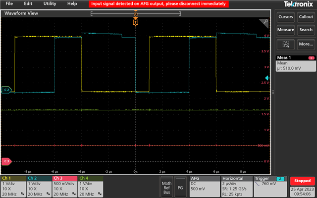
EPWM3A tests is as below.

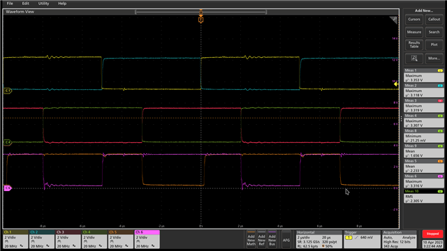
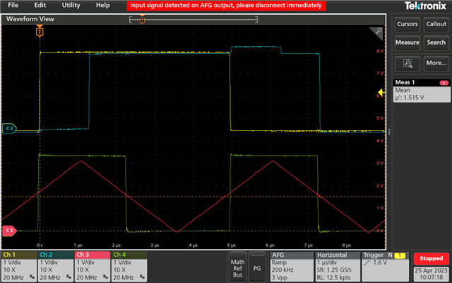
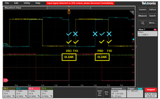
Case #1:  I want to see ORing of EPWM1A and 2B and monitor ORing for ePWM3A. I write 0 to RAMPMAXREF of CMPSS and see minimum duty case.
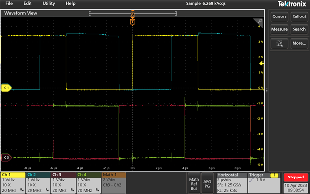
YELLOW:ePWM1A,  GREEN: ePWM2B, BLUE: ePWM3A

I don't get stable waveforms at ePWM3A. It should rise to high when ePWM1A is high. The position of rise of ePWM3A varies when I change .

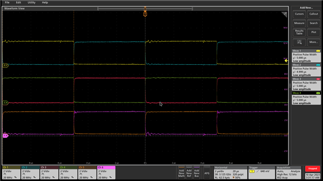
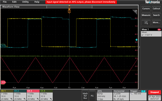
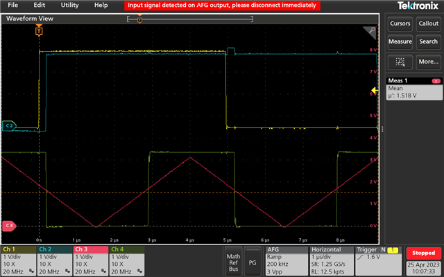
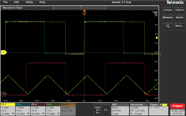
Case #2: In below lines, I provided external ramp signal to my ADC port. I wrote 32767 as CMPSS max ramp value. I got following waveforms, which also shows instability at ePWM3A.
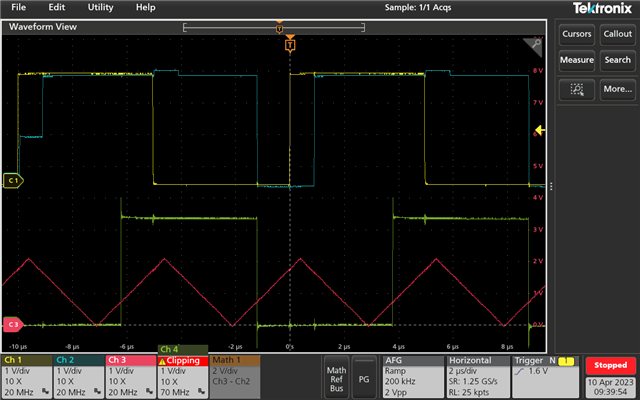
YELLOW:ePWM1A,  GREEN: ePWM2B, BLUE: ePWM3A, RED: External Ramp Signal to CMPSS

EPWM3B tests is as below.

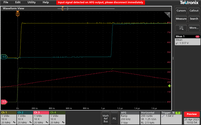
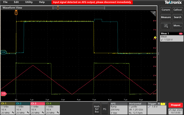
Case #3: I want to see ORing of EPWM1B and 2A and monitor ORing for ePWM3B. I write 0 to RAMPMAXREF of CMPSS and see minimum duty case.

It works fine.
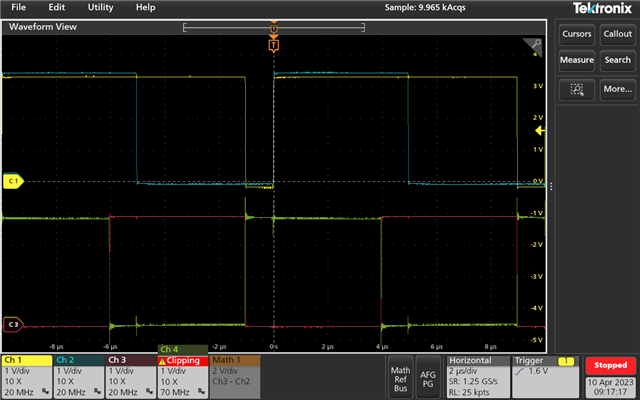
BLUE: ePWM1B,    RED: ePWM2A,     GREEN: ePWM2B,  YELLOW:ePWM3B, 

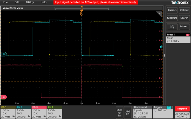
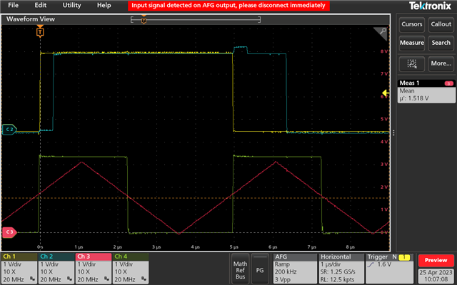
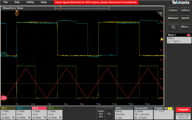
CASE 4: I provided external same ramp signal as above and monitored whether ePWM3B follows it or not.
YELLOW:ePWM3B,  BLUE: ePWM1B,  RED: ePWM2A,  GREEN: external RAMP signal,

Waveform is as expected at ePWM3B. 3B follows to the events. It is fine.

I provided same blanking window timings on for both 1A and 1B and 3A and 3B.

Could you please comment how ePWM3A doesn't follow the event although ePWM3B follows the same event? How can ı fix it?

Why does ePWM3A has instable signals, I also can provide video.

Thank you in advance.

  • Hi,

    I also loaded the same software to my board, which has F280048. 

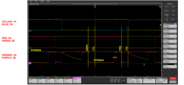
    I got following waveform as I described at case #1. At minimum duty, my ePWM3A has some problems as you can see.

    YELLOW: 1A, BLUE: 1B,                     RED: 2A, GREEN:2B,               ORANGE:3A, PURPLE 3B

    At below, I changed ADCIN value by using potentiometer and I loaded deadbands as zero. Please check below waveform it isn't as expected considering dead-band.

    Deadtime isn't zero at ePWM3A and however, now, it can follow the ORing of 1A and 2B.

    In below, I changed voltage value at ADCIN using potentiometer, at %100 duty the waveforms seems OK. 

    Could you please help on it? My ePWM3A has some strange characteristics at demoboard and also on my board. However, ePWM3B works as expected.

    Thank you.

  • Since EPWM3B is behaving as expected, I would assume the comparator output is getting routed to EPWM3 correctly. Then perhaps there is an issue with the action qualifier configuration for EPWM3A. Can you share that piece of code? 

  • Hi Gus,

    I added it as below. 

        // Action-Qualifier Submodule Configurations
        // ePWM3A Actions
        // CTR = ZERO , set to 0
        // CTR = PRD , set to 1
        // CTR = T1U , set to 1
        // CTR = T1D , set to 1
        //
        EPWM_setActionQualifierAction(EPWM3_BASE,EPWM_AQ_OUTPUT_A,EPWM_AQ_OUTPUT_LOW,
                                      EPWM_AQ_OUTPUT_ON_TIMEBASE_ZERO);
        EPWM_setActionQualifierAction(EPWM3_BASE,EPWM_AQ_OUTPUT_A,EPWM_AQ_OUTPUT_HIGH,
                                      EPWM_AQ_OUTPUT_ON_TIMEBASE_PERIOD);
        EPWM_setActionQualifierAction(EPWM3_BASE,EPWM_AQ_OUTPUT_A,EPWM_AQ_OUTPUT_NO_CHANGE,
                                      EPWM_AQ_OUTPUT_ON_TIMEBASE_UP_CMPA);
        EPWM_setActionQualifierAction(EPWM3_BASE,EPWM_AQ_OUTPUT_A,EPWM_AQ_OUTPUT_NO_CHANGE,
                                      EPWM_AQ_OUTPUT_ON_TIMEBASE_DOWN_CMPA);
        EPWM_setActionQualifierAction(EPWM3_BASE,EPWM_AQ_OUTPUT_A,EPWM_AQ_OUTPUT_NO_CHANGE,
                                      EPWM_AQ_OUTPUT_ON_TIMEBASE_UP_CMPB);
        EPWM_setActionQualifierAction(EPWM3_BASE,EPWM_AQ_OUTPUT_A,EPWM_AQ_OUTPUT_NO_CHANGE,
                                      EPWM_AQ_OUTPUT_ON_TIMEBASE_DOWN_CMPB);
        EPWM_setActionQualifierAction(EPWM3_BASE,EPWM_AQ_OUTPUT_A,EPWM_AQ_OUTPUT_HIGH,
                                      EPWM_AQ_OUTPUT_ON_T1_COUNT_UP);
        EPWM_setActionQualifierAction(EPWM3_BASE,EPWM_AQ_OUTPUT_A,EPWM_AQ_OUTPUT_HIGH,
                                      EPWM_AQ_OUTPUT_ON_T1_COUNT_DOWN);

    As you can see at Case #1, the amplitude of the PWM signal is also changes in cycle. Also in my own board case, the power drawn from power supply also increases when I change the potentiometer and change the voltage of ADCIN pin. It seemed me when I change the ADCIN voltage, somethings drives inside ePWM3A module.

    I also added blanking window and timebase lines as below.

        EPWM_setDigitalCompareWindowOffset(EPWM1_BASE, PeriodValue - 100);
    
        // Set the blanking window length in TBCLK counts
        // 10*TBLCK = 100nsec
        EPWM_setDigitalCompareWindowLength(EPWM1_BASE, 200);    
        
        //
        // Configure PWM1 as master
        //
        EPWM_disablePhaseShiftLoad(EPWM1_BASE);
        EPWM_setSyncOutPulseMode(EPWM1_BASE, EPWM_SYNC_OUT_PULSE_ON_COUNTER_ZERO);

        EPWM_setDigitalCompareWindowOffset(EPWM3_BASE, PeriodValue - 100);
    
        // Set the blanking window length in TBCLK counts
        // 10*TBLCK = 100nsec
        EPWM_setDigitalCompareWindowLength(EPWM3_BASE, 200);
        
        EPWM_enablePhaseShiftLoad(EPWM3_BASE);
        EPWM_setSyncOutPulseMode(EPWM3_BASE, EPWM_SYNC_OUT_PULSE_ON_EPWMxSYNCIN);
    
        EPWM_setPhaseShift(EPWM3_BASE, 2); // Value*TBCLKs Phase-Shift is Set
        EPWM_setCountModeAfterSync(EPWM3_BASE, EPWM_COUNT_MODE_UP_AFTER_SYNC);

  • As you can see at Case #1, the amplitude of the PWM signal is also changes in cycle. Also in my own board case, the power drawn from power supply also increases when I change the potentiometer and change the voltage of ADCIN pin. It seemed me when I change the ADCIN voltage, somethings drives inside ePWM3A module.

    The only thing I can think of is that there is some noise coupling into the PWM pins from another source. Is the LaunchPad fully disconnected from any power stage (inductors, FETs, transformer shown in your diagram)? Can you replicate this issue by using any of the standard C2000ware PWM examples? If so, we may be able to replicate on our end.

    I added it as below. 

    OK, the action qualifier code looks ok to me. Are you also separately configuring the trip zone module to force a state on the PWM outputs? 

  • Hi Gus, Thank you for help.

    Can you replicate this issue by using any of the standard C2000ware PWM examples?

    I generally designed software using example reference software, you can guide me which software I should use to download my demoboard. By the way, I can send my source code via e-mail on our local distributor. In this way, you can also replicate it.

    Waveforms at my first post are taken from demoboard F280049C in that case there is no power component. I have header wires to monitor the signals. I externally provide ramp signal from oscilloscope output.

    Waveforms at my second post are taken from my own board in that case there are power components. I externally provide DC signals using potentiometer.

    Are you also separately configuring the trip zone module to force a state on the PWM outputs?

    It is as below;

    For ePWM1, it is as below;

    //
        // Set DCEVTFILT as the trigger source for Channel A
        //
        EPWM_setActionQualifierT1TriggerSource(EPWM1_BASE,
                                               EPWM_AQ_TRIGGER_EVENT_TRIG_DC_EVTFILT);
    
        // Digital Compare and Comparator-X-Bar Configuration
        // Disable all the muxes first
        XBAR_enableEPWMMux(XBAR_TRIP4, 0x00);
    
        //
        // Setup PWM TRIP 4 as the destination for CMPSS5H output (PCMC)
        // TRIP4 will be ACTIVE if CTRIPH is HIGH at CMPSS5
        XBAR_setEPWMMuxConfig(XBAR_TRIP4, XBAR_EPWM_MUX08_CMPSS5_CTRIPH);
        XBAR_enableEPWMMux(XBAR_TRIP4, XBAR_MUX08);
    
        //
        // DCAH = TRIP5 = Comparator 1H output
        //
        EPWM_selectDigitalCompareTripInput(EPWM1_BASE, EPWM_DC_TRIP_TRIPIN4,
                                            EPWM_DC_TYPE_DCAH);
    
        //
        // DCAH = high
        //
        EPWM_setTripZoneDigitalCompareEventCondition(EPWM1_BASE, EPWM_TZ_DC_OUTPUT_A2,
                                            EPWM_TZ_EVENT_DCXH_HIGH);
    
        //
        // Set the source for digital compare filter as DCAEVT2
        //
        EPWM_setDigitalCompareEventSource(EPWM1_BASE, EPWM_DC_MODULE_A,EPWM_DC_EVENT_2,
                                          EPWM_DC_EVENT_SOURCE_FILT_SIGNAL);
    
        // Allow ASYNC DCAEVT2 for trip zone actions
        EPWM_setDigitalCompareEventSyncMode(EPWM1_BASE, EPWM_DC_MODULE_A,
                                            EPWM_DC_EVENT_2,
                                            EPWM_DC_EVENT_INPUT_NOT_SYNCED);
    
        // Select DCAEVT2 cycle by cycle trip
        EPWM_enableTripZoneSignals(EPWM1_BASE, EPWM_TZ_SIGNAL_DCAEVT2);
    
        //
        // Event Filtering Configuration (inside digital compare)
        // Enable DC filter blanking window
        //
        EPWM_enableDigitalCompareBlankingWindow(EPWM1_BASE);
    
        // Set the signal source that will be filtered.
        EPWM_setDigitalCompareFilterInput(EPWM1_BASE, EPWM_DC_WINDOW_SOURCE_DCAEVT2);
    
        // Set the Digital Compare filter blanking pulse.
        EPWM_setDigitalCompareBlankingEvent(EPWM1_BASE,
                                         EPWM_DC_WINDOW_START_TBCTR_ZERO_PERIOD);
    
        // Set the blanking window offset in TBCLK counts
        // An offset value in TBCLK counts is programmed
        // which determines at what point aft<er the CTR = PRD or CTR = 0 pulse the blanking window starts.
        EPWM_setDigitalCompareWindowOffset(EPWM1_BASE, PeriodValue - 100);
    
        // Set the blanking window length in TBCLK counts
        // 10*TBLCK = 100nsec
        EPWM_setDigitalCompareWindowLength(EPWM1_BASE, 200);
    
        //
        // Trip-zone event actions
        // What do we want the CBC events to do?
        // TZAx events can force EPWMxA
        // TZBx events can force EPWMxB
        //
        EPWM_setTripZoneAdvAction(EPWM1_BASE, EPWM_TZ_ADV_ACTION_EVENT_TZA_D,
                                  EPWM_TZ_ADV_ACTION_LOW);
        EPWM_setTripZoneAdvAction(EPWM1_BASE, EPWM_TZ_ADV_ACTION_EVENT_TZA_U,
                                  EPWM_TZ_ADV_ACTION_DISABLE);
        EPWM_setTripZoneAdvAction(EPWM1_BASE, EPWM_TZ_ADV_ACTION_EVENT_TZB_U,
                                  EPWM_TZ_ADV_ACTION_LOW);
        EPWM_setTripZoneAdvAction(EPWM1_BASE, EPWM_TZ_ADV_ACTION_EVENT_TZB_D,
                                  EPWM_TZ_ADV_ACTION_DISABLE);
        EPWM_setTripZoneAction(EPWM1_BASE, EPWM_TZ_ACTION_EVENT_TZA,
                               EPWM_TZ_ACTION_DISABLE);
        EPWM_setTripZoneAction(EPWM1_BASE, EPWM_TZ_ACTION_EVENT_TZB,
                               EPWM_TZ_ACTION_DISABLE);
        //
        // Select CBC clear event
        EPWM_selectCycleByCycleTripZoneClearEvent(EPWM1_BASE,
                               EPWM_TZ_CBC_PULSE_CLR_CNTR_ZERO_PERIOD);
        //
        // Clear any spurious trip
        EPWM_clearTripZoneFlag(EPWM1_BASE, (EPWM_TZ_INTERRUPT_OST |
                EPWM_TZ_INTERRUPT_DCAEVT2 | EPWM_TZ_SIGNAL_DCBEVT1));
        EPWM_clearTripZoneFlag(EPWM2_BASE, (EPWM_TZ_INTERRUPT_OST |
                EPWM_TZ_INTERRUPT_DCAEVT2 | EPWM_TZ_SIGNAL_DCBEVT1));
    
        //
        // Dead-Band Submodule Configuration
        //
        EPWM_setDeadBandCounterClock(EPWM1_BASE, EPWM_DB_COUNTER_CLOCK_FULL_CYCLE);
        EPWM_setRisingEdgeDelayCount(EPWM1_BASE, 10);
        EPWM_setFallingEdgeDelayCount(EPWM1_BASE, 10);
    
        //DelayMode select
        //EPWM_DB_RED   - Rising Edge delay,
        //EPWM_DB_FED   - Falling Edge delay
        //true     - Falling edge or Rising edge delay is applied.
        //false    - Dead Band delay is bypassed.
        EPWM_setDeadBandDelayMode(EPWM1_BASE, EPWM_DB_RED, true);
        EPWM_setDeadBandDelayMode(EPWM1_BASE, EPWM_DB_FED, true);
        EPWM_setRisingEdgeDeadBandDelayInput(EPWM1_BASE, EPWM_DB_INPUT_EPWMA);
        EPWM_setFallingEdgeDeadBandDelayInput(EPWM1_BASE, EPWM_DB_INPUT_EPWMB);
    
        // xA is RED, same!!!
        // xB is FED, inverted (AHC) !!!
        EPWM_setDeadBandDelayPolarity(EPWM1_BASE, EPWM_DB_RED, EPWM_DB_POLARITY_ACTIVE_HIGH);
        EPWM_setDeadBandDelayPolarity(EPWM1_BASE, EPWM_DB_FED, EPWM_DB_POLARITY_ACTIVE_LOW);
    
        //
        // Configure PWM1 as master
        //
        EPWM_disablePhaseShiftLoad(EPWM1_BASE);
        EPWM_setSyncOutPulseMode(EPWM1_BASE, EPWM_SYNC_OUT_PULSE_ON_COUNTER_ZERO);
    
        EDIS;

    For ePWM3, it is as below;

    //
        // Set DCEVTFILT as the trigger source for Channel A
        //
        EPWM_setActionQualifierT1TriggerSource(EPWM3_BASE,
                                              EPWM_AQ_TRIGGER_EVENT_TRIG_DC_EVTFILT);
    
        //
        // Digital Compare Configuration
        // DCAH = TRIP4 = Comparator 1 output (high side)
        //
        EPWM_selectDigitalCompareTripInput(EPWM3_BASE, EPWM_DC_TRIP_TRIPIN4,
                                          EPWM_DC_TYPE_DCAH);
    
        //
        // DCAH = high
        //
        EPWM_setTripZoneDigitalCompareEventCondition(EPWM3_BASE, EPWM_TZ_DC_OUTPUT_A2,
                                                    EPWM_TZ_EVENT_DCXH_HIGH);
    
        //
        // Set the source for digital compare filter as DCAEVT2
        //
        EPWM_setDigitalCompareEventSource(EPWM3_BASE, EPWM_DC_MODULE_A, EPWM_DC_EVENT_2,
                                         EPWM_DC_EVENT_SOURCE_FILT_SIGNAL);
    
        //
        // Allow ASYNC DCAEVT2 for trip zone actions
        //
        EPWM_setDigitalCompareEventSyncMode(EPWM3_BASE, EPWM_DC_MODULE_A,
                                           EPWM_DC_EVENT_2,
                                           EPWM_DC_EVENT_INPUT_NOT_SYNCED);
    
        // Event Filtering Configuration (inside digital compare)
        // Enable DC filter blanking window
        //
        EPWM_enableDigitalCompareBlankingWindow(EPWM3_BASE);
    
        //
        // Set the signal source that will be filtered.
        //
        EPWM_setDigitalCompareFilterInput(EPWM3_BASE, EPWM_DC_WINDOW_SOURCE_DCAEVT2);
    
        //
        // Set the Digital Compare filter blanking pulse.
        //
        EPWM_setDigitalCompareBlankingEvent(EPWM3_BASE,
                                           EPWM_DC_WINDOW_START_TBCTR_ZERO_PERIOD);
    
        // Set the blanking window offset in TBCLK counts
        // An offset value in TBCLK counts is programmed
        // which determines at what point after the CTR = PRD or CTR = 0 pulse the blanking window starts.
        EPWM_setDigitalCompareWindowOffset(EPWM3_BASE, PeriodValue - 100);
    
        // Set the blanking window length in TBCLK counts
        // 10*TBLCK = 100nsec
        EPWM_setDigitalCompareWindowLength(EPWM3_BASE, 200);
    
    
        EPWM_setDeadBandControlShadowLoadMode(EPWM3_BASE, EPWM_DB_LOAD_ON_CNTR_ZERO);
    
        EPWM_setDeadBandCounterClock(EPWM3_BASE, EPWM_DB_COUNTER_CLOCK_FULL_CYCLE);
        EPWM_setRisingEdgeDelayCount(EPWM3_BASE, 35);
        EPWM_setFallingEdgeDelayCount(EPWM3_BASE, 35);
        EPWM_setDeadBandDelayMode(EPWM3_BASE, EPWM_DB_RED, true);
        EPWM_setDeadBandDelayMode(EPWM3_BASE, EPWM_DB_FED, true);
        EPWM_setRisingEdgeDeadBandDelayInput(EPWM3_BASE, EPWM_DB_INPUT_EPWMA);
        EPWM_setFallingEdgeDeadBandDelayInput(EPWM3_BASE, EPWM_DB_INPUT_EPWMB);
        EPWM_setDeadBandDelayPolarity(EPWM3_BASE, EPWM_DB_RED,
                                      EPWM_DB_POLARITY_ACTIVE_HIGH);
    
        //
        // xB is inverted
        //
        EPWM_setDeadBandDelayPolarity(EPWM3_BASE, EPWM_DB_FED,
                                      EPWM_DB_POLARITY_ACTIVE_LOW);
    
        //
        // Phase Configuration and Set
        // Configure PWM base3 as slave
        // SetPhaseShift = Value*TBCLK = Value*10nsec
        EPWM_enablePhaseShiftLoad(EPWM3_BASE);
        EPWM_setSyncOutPulseMode(EPWM3_BASE, EPWM_SYNC_OUT_PULSE_ON_EPWMxSYNCIN);
    
        EPWM_setPhaseShift(EPWM3_BASE, 2); // Value*TBCLKs Phase-Shift is Set
        EPWM_setCountModeAfterSync(EPWM3_BASE, EPWM_COUNT_MODE_UP_AFTER_SYNC);
    
    
        EDIS;

    Thanks in advance, Gus.

  • I generally designed software using example reference software, you can guide me which software I should use to download my demoboard. By the way, I can send my source code via e-mail on our local distributor. In this way, you can also replicate it.

    It is generally easier to debug an issue on TI provided SW examples if the issue can be replicated since our internal support teams are more familiar with that firmware. You can leverage the EPWM examples in C2000ware. It looks like epwm_ex2_updown_aq may be of use. The goal here is to run this example as-is on your LaunchPad and see if the PWM amplitude issue is there as well. If it is, then we can take a look. 

    C:\ti\c2000\C2000Ware_4_03_00_00\driverlib\f28004x\examples\epwm

    For ePWM3, it is as below;

    I'm still going through your EPWM3 configuration. It will get back to you in a couple of days.

  • Gokhan,

    I reviewed your PWM3 configuration. Here you are setting the dead band module (DBM) RED input to the AQ PWMA output and the FED input to the AQ PWMB output. This is totally fine, however, in your PWM3 configuration I don't see where you control the AQ PWMB output. In previous calls to EPWM_setActionQualifierAction(), I only see actions on EPWM_AQ_OUTPUT_A. Do you have AQ configuration for EPWM_AQ_OUTPUT_B?

        EPWM_setRisingEdgeDeadBandDelayInput(EPWM3_BASE, EPWM_DB_INPUT_EPWMA);
        EPWM_setFallingEdgeDeadBandDelayInput(EPWM3_BASE, EPWM_DB_INPUT_EPWMB);

  • Apologies, I just realized I didn't ask for AQ EPWMB configuration, so maybe that's the reason you didn't include it here on this thread. 

    In any case, I took a closer look at one of your graphs:

    Actually EPWM3B looks ok to me. It is EPWM3A that doesn't look right: 

    • EPWM3A maybe going into high-z for some cycles.
    • EPWM3A is reacting to some event which doesn't seem to line up with any of the other EPWM edges

    I would focus there.

    Some debug things you could do:

    • Bypass the DBM entirely. 

        EPWM_setDeadBandDelayMode(EPWM3_BASE, EPWM_DB_RED, false);
        EPWM_setDeadBandDelayMode(EPWM3_BASE, EPWM_DB_FED, false);

    This should the set the PWMA and PWMB pins to be sourced directly from the AQ module. Maybe this will offer some clues as to whether the configuration issue is with the AQ or the DBM.

    • Route the CMPSS trip output to a GPIO pin using the OUTPUT XBAR.

    This will allow you to see if the CMPSS is maybe generating multiple events. 

  • Hi Gus,

    Thank you for feedback. I will try and inform you about the issue.

    Configuration for ePWM3B is as below.

        // Action-Qualifier Submodule Configurations
        // ePWM3B Actions
        // CTR = ZERO , set to 0
        // CTR = PRD , set to 1
        // CTR = T1U , set to 0
        // CTR = T1D , set to 0
        EPWM_setActionQualifierAction(EPWM3_BASE,EPWM_AQ_OUTPUT_B,EPWM_AQ_OUTPUT_LOW,
                                      EPWM_AQ_OUTPUT_ON_TIMEBASE_ZERO);
        EPWM_setActionQualifierAction(EPWM3_BASE,EPWM_AQ_OUTPUT_B,EPWM_AQ_OUTPUT_HIGH,
                                      EPWM_AQ_OUTPUT_ON_TIMEBASE_PERIOD);
        EPWM_setActionQualifierAction(EPWM3_BASE,EPWM_AQ_OUTPUT_B,EPWM_AQ_OUTPUT_NO_CHANGE,
                                      EPWM_AQ_OUTPUT_ON_TIMEBASE_UP_CMPA);
        EPWM_setActionQualifierAction(EPWM3_BASE,EPWM_AQ_OUTPUT_B,EPWM_AQ_OUTPUT_NO_CHANGE,
                                      EPWM_AQ_OUTPUT_ON_TIMEBASE_DOWN_CMPA);
        EPWM_setActionQualifierAction(EPWM3_BASE,EPWM_AQ_OUTPUT_B,EPWM_AQ_OUTPUT_NO_CHANGE,
                                      EPWM_AQ_OUTPUT_ON_TIMEBASE_UP_CMPB);
        EPWM_setActionQualifierAction(EPWM3_BASE,EPWM_AQ_OUTPUT_B,EPWM_AQ_OUTPUT_NO_CHANGE,
                                      EPWM_AQ_OUTPUT_ON_TIMEBASE_DOWN_CMPB);
        EPWM_setActionQualifierAction(EPWM3_BASE,EPWM_AQ_OUTPUT_B,EPWM_AQ_OUTPUT_LOW,
                                      EPWM_AQ_OUTPUT_ON_T1_COUNT_UP);
        EPWM_setActionQualifierAction(EPWM3_BASE,EPWM_AQ_OUTPUT_B,EPWM_AQ_OUTPUT_LOW,
                                      EPWM_AQ_OUTPUT_ON_T1_COUNT_DOWN);

  • Hi Gus,

    As a reminder, I use Inverted+FED at ePWM3B.

    Could you generate the same issue at your own test board?

  • Hi Gus,

    I did below tests using demoboard of LAUNCHXL-F280049C. I will also try it at my own board. Characteristic differs from 49C demoboard to 48 own board but similar.

    This is the baseline waveform before changing the software based on your offers. I used same colours at probing.

    YELLOW:ePWM1ARED:ePWM2A, GREEN: ePWM2B, BLUE: ePWM3A

    1) I bypassed DBM as you offered. I got following waveform.

    YELLOW:ePWM1A RED:ePWM2A, GREEN: ePWM2B, BLUE: ePWM3A

    2) I routed CMPSS output to OUTPUT X-BAR. It is RED as below.

    //
    // Monitoring via OUTPUTXBAR
    //
    void Outputxbar_to_monitorCMPSSOUT(void)
    {
        //myOUTPUTXBAR0 initialization
        XBAR_setOutputLatchMode(XBAR_OUTPUT3, false);
        XBAR_invertOutputSignal(XBAR_OUTPUT3, false);
    
        //Mux configuration
        XBAR_setOutputMuxConfig(XBAR_OUTPUT3, XBAR_OUT_MUX08_CMPSS5_CTRIPOUTH);
        XBAR_enableOutputMux(XBAR_OUTPUT3, XBAR_MUX08);
    }
    
    void PinMux_init(void)
    {
        GPIO_setPinConfig(GPIO_26_OUTPUTXBAR3);
    }
    

    TEST#1: I wrote 0 to both REF_CMPSS_PEAK and PSFB_SLOPE_INITIAL. I didn't apply any signal to ADCIN port which is internally connected to CMPSS. I got below waveform. 

    YELLOW:ePWM1A RED:ePWM2A, GREEN: CMPSSOUT-XBAR , BLUE: ePWM3A

    TEST#2: I provided 0.5VDC to ADCIN signal. I didn't change CMPSS set values. REF_CMPSS_PEAK =0, PSFB_SLOPE_INITIAL=0

    YELLOW:ePWM1A RED: External Signal to ADCIN, GREEN: CMPSSOUT-XBAR , BLUE: ePWM3A


    TEST#3: I provided ramp signal 0-3V at 200khz with %50 symmetry. REF_CMPSS_PEAK =0, PSFB_SLOPE_INITIAL=0 is still same.

    YELLOW:ePWM1A RED: External Signal to ADCIN, GREEN: CMPSSOUT-XBAR , BLUE: ePWM3A

    TEST#4: I provided ramp signal 0-3V at 200khz with %50 symmetry in RED waveform. REF_CMPSS_PEAK =32676, PSFB_SLOPE_INITIAL=0 is applied.

    YELLOW:ePWM1A RED: External Signal to ADCIN, GREEN: CMPSSOUT-XBAR , BLUE: ePWM3A

    When I focused I got following waveform.

    YELLOW:ePWM1A RED: External Signal to ADCIN, GREEN: CMPSSOUT-XBAR , BLUE: ePWM3A

    My external signal isn't synchronized to PWM's so the invent instants varies in time. I captured some waveforms only stopping the waveform at different instants using single feature of oscilloscope.

    YELLOW:ePWM1A RED: External Signal to ADCIN, GREEN: CMPSSOUT-XBAR , BLUE: ePWM3A

    YELLOW:ePWM1A RED: External Signal to ADCIN, GREEN: CMPSSOUT-XBAR , BLUE: ePWM3A

    At above, we have same events but different reaction instants on ePWM3A !!! It isn't as expected.

    However, ePWM3A catches T1D event really nice and gets low.

    YELLOW:ePWM1A RED: External Signal to ADCIN, GREEN: CMPSSOUT-XBAR , BLUE: ePWM3A

    An also interesting waveform as below. When OutputXbar goes low, ePWM3A rises to high. Maybe it is just a coincidence.

    YELLOW:ePWM1A RED: External Signal to ADCIN, GREEN: CMPSSOUT-XBAR , BLUE: ePWM3A

    Beacuse it isn't always same as below. 

    YELLOW:ePWM1A RED: External Signal to ADCIN, GREEN: CMPSSOUT-XBAR , BLUE: ePWM3A

    I didn't observe any glitches or different timings at CMPSS output. Waveforms at CMPSSOUT seems nice. Something inside affects ePWM3A.

    My observation is as below:

    ePWM3A output is affected by CMPSS signal inside. ePWM3A rises to high when comparators output has high-to-low transition. You can see some waveforms at above. But it isn't stable operation, because I also could capture the following waveform as expected.

    At an instant it is OK, but in other cycle it is NOK.

  • This is great. Now we have a lot more stuff to look at. Here is what I can see.

    In Test #1 & Test #2, since the CMPSS output is always high, you will be continuously generating the one-shot trip event for EPWM1A/1B. This means that T1U and T1D will be immediately generated after ZRO and PRD resets the trip event. I believe there is a slight delay here because of your blanking window configuration. If you vary that blanking window or set it to zero you should see EPWM1A/1B start to approximate EPWM2A/2B. However, see note at the bottom of this post.

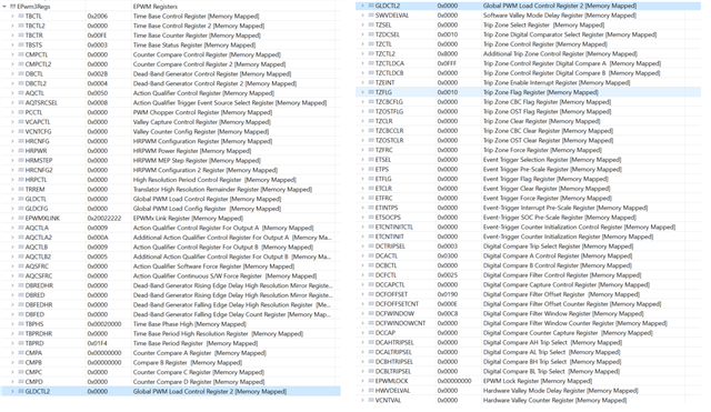
    EPWM3A is reacting to some unknown event. It seems related to the blanking window though. Are you sure you are not configuring the Trip Zone actions on EPWM3A? Can you check the EPWM3 registers after you load your code? Those pulses EPWM3A seem to indicate the pin is going to high-z. Do you have pull-ups enabled on the GPIO config for this pin? Or do you have an external pull-up on this pin? 

    On Test #4, EPWM1A is completely in sync with CMPSSOUT-XBAR, which doesn't make sense to me. The blanking window should apply here as well. I cannot explain why this is happening. Did the blanking window configuration change for this test? 

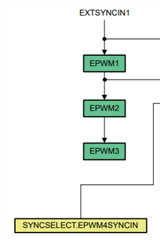
    I also noticed one more thing. Why did you decide to make EPWM2 the master? Based on the F280049C architecture, EPWM2 cannot SYNC EPWM1. This means it is possible for EPWM1 and EPWM2 to be out of sync with each other. 

  • I just had a realization. The TZCTL and TZCTLDCA registers also have fields that specify the trip-zone action on DCAEVT2 (the digital compare signal you have used to trip EPWM3). By default, TZCTL.DCAEVT2=00 specifies the EPWM3A pin should go to high-z on DCAEVT2. Similarly for TZCTLDCA.DCAEVT2D=000 and TZCTLDCA.DCAEVT2U=000 (trip action on DCAEVT2 count up and count down). Can you confirm this is the case on your end? Can you try changing these to the "do nothing" action (11b and 111b respectively). 

  • Hi Gus,

    There is really happy news at my side. You fixed my problem. I really appreciated your guide.Blush

    I just added below lines to my ePWM3 init. Now, ePWM3A follows ePWM1A very well at rise instants. I tested it by using Launchxl-F2800049C. I performed all test cases at above, it is OK. I will also try it at my own board and send you waveform.

        EPWM_setTripZoneAdvDigitalCompareActionA(EPWM3_BASE, EPWM_TZ_ADV_ACTION_EVENT_DCxEVT2_D,
                                                 EPWM_TZ_ADV_ACTION_DISABLE);
        EPWM_setTripZoneAdvDigitalCompareActionA(EPWM3_BASE, EPWM_TZ_ADV_ACTION_EVENT_DCxEVT2_U,
                                                 EPWM_TZ_ADV_ACTION_DISABLE);
        EPWM_setTripZoneAdvDigitalCompareActionA(EPWM3_BASE, EPWM_TZ_ADV_ACTION_EVENT_DCxEVT1_D,
                                                 EPWM_TZ_ADV_ACTION_DISABLE);
        EPWM_setTripZoneAdvDigitalCompareActionA(EPWM3_BASE, EPWM_TZ_ADV_ACTION_EVENT_DCxEVT1_U,
                                                 EPWM_TZ_ADV_ACTION_DISABLE);

    I added waveforms as below. It seems OK.

    YELLOW:ePWM1A,  RED: External Signal to ADCIN, GREEN: CMPSSOUT-XBAR , BLUE: ePWM3A

    However, I wonder that WHY example software doesn't have those lines. Do you have any idea?

    I also commented your concerns as below.

    Are you sure you are not configuring the Trip Zone actions on EPWM3A? Can you check the EPWM3 registers after you load your code? Those pulses EPWM3A seem to indicate the pin is going to high-z. Do you have pull-ups enabled on the GPIO config for this pin? Or do you have an external pull-up on this pin?

    I didn't have had trip zone lines at my ePWM3 software I just had it for ePWM1. I just configure ePWM3 output as other ePWM1 and 2 lines. I don't have external pull-up resistors at my board.

        GPIO_setMasterCore(4, GPIO_CORE_CPU1);
        GPIO_setPinConfig(GPIO_4_EPWM3_A);
        GPIO_setDirectionMode(4, GPIO_DIR_MODE_OUT);
        GPIO_setPadConfig(4, GPIO_PIN_TYPE_STD);
        GPIO_setQualificationMode(4, GPIO_QUAL_ASYNC);
    
        GPIO_setMasterCore(5, GPIO_CORE_CPU1);
        GPIO_setPinConfig(GPIO_5_EPWM3_B);
        GPIO_setDirectionMode(5, GPIO_DIR_MODE_OUT);
        GPIO_setPadConfig(5, GPIO_PIN_TYPE_STD);
        GPIO_setQualificationMode(5, GPIO_QUAL_ASYNC);

    Register screen is shown at below for before and after including CORRECT Lines.

    BEFORE

    AFTER

    On Test #4, EPWM1A is completely in sync with CMPSSOUT-XBAR, which doesn't make sense to me. The blanking window should apply here as well. I cannot explain why this is happening. Did the blanking window configuration change for this test?

    Actually, it is as expected at my side. Because, when CMPSSOUT-XBAR is high, T1 event is generated and ePWM1 follows it and gets high. My external signal provided to the ADCIN isn't synchoronized to my ePWM timebase. I generated external ramp signal from oscilloscope and times that CMPSS OUT rises to high differs in time. I just run/stop the oscilloscope to capture some intervals.

    I also noticed one more thing. Why did you decide to make EPWM2 the master? Based on the F280049C architecture, EPWM2 cannot SYNC EPWM1. This means it is possible for EPWM1 and EPWM2 to be out of sync with each other. 

    I use ePMW1 as master and others as slave. However, I changed the switching topology according to Tr-Lead or Tr-Lag. In phase-shifted topology, the switch that ends power transfer interval may differ and improve efficiency when external clamping diodes are used. This is beacause why I changed the event based ePWM. In example software, it is ePWM2. My software lines for sync is as below. Can you confirm?

        EPWM_disablePhaseShiftLoad(EPWM1_BASE);
        EPWM_setSyncOutPulseMode(EPWM1_BASE, EPWM_SYNC_OUT_PULSE_ON_COUNTER_ZERO);
        
        EPWM_enablePhaseShiftLoad(EPWM2_BASE);
        EPWM_setSyncOutPulseMode(EPWM2_BASE, EPWM_SYNC_OUT_PULSE_ON_EPWMxSYNCIN);
        EPWM_setPhaseShift(EPWM2_BASE, 2);
        EPWM_setCountModeAfterSync(EPWM2_BASE, EPWM_COUNT_MODE_UP_AFTER_SYNC);
        
        EPWM_enablePhaseShiftLoad(EPWM3_BASE);
        EPWM_setSyncOutPulseMode(EPWM3_BASE, EPWM_SYNC_OUT_PULSE_ON_EPWMxSYNCIN);
        EPWM_setPhaseShift(EPWM3_BASE, 2);
        EPWM_setCountModeAfterSync(EPWM3_BASE, EPWM_COUNT_MODE_UP_AFTER_SYNC);

    I can try some more things at demoboard if you wish.

  • There is really happy news at my side. You fixed my problem.

    That's awesome!

    However, I wonder that WHY example software doesn't have those lines. Do you have any idea?

    This is a bit of mystery to me as well. I will need to check with the original code developers. However, that may take a while. In any case, glad we were able to solve it here!

    I use ePMW1 as master and others as slave. However, I changed the switching topology according to Tr-Lead or Tr-Lag. In phase-shifted topology, the switch that ends power transfer interval may differ and improve efficiency when external clamping diodes are used. This is beacause why I changed the event based ePWM. In example software, it is ePWM2. My software lines for sync is as below. Can you confirm?

    I am not sure I follow your reasoning entirely. However, as long as the three PWMs are in sync with each other, I think it should be ok. Your configuration looks ok to me.