This thread has been locked.

If you have a related question, please click the "Ask a related question" button in the top right corner. The newly created question will be automatically linked to this question.

TMS320F280049: unexpected pulse at slave epwm2.

Part Number: TMS320F280049
Other Parts Discussed in Thread: SYSCONFIG

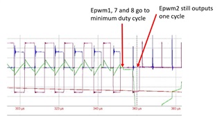
unexpected pulse at epwm2.

The configuration that we have done is: 

Epwm1 is the master of epwm2, 7 and 8

All work with phase 0

Their periods are all sync with TBPRDLINK.

GLDMODE is done when the counter reaches Z(0).

All are configured in one shot mode OSHTMODE=1

We change the pwm CMPA and CMPB registers dynamically from a CLA task synchronized with the period of the pwm

we have observed that occasionally, when changing from a certain on time (something like 40% duty cycle) to a very low value (t1_cnts and t2_cnts lower than the deadtime), epwm2 takes one extra cycle to output that value, while all other modules do it immediately.

  • Please find here the pwm.c source file (TI internal link, not accessible publicly).

    Thank you.


    François.

  • Hi Francois and Nada, 

    we have observed that occasionally, when changing from a certain on time (something like 40% duty cycle) to a very low value (t1_cnts and t2_cnts lower than the deadtime), epwm2 takes one extra cycle to output that value, while all other modules do it immediately.

    Are you able to provide a scope capture of this issue while I review the file attached?

    We change the pwm CMPA and CMPB registers dynamically from a CLA task synchronized with the period of the pwm

    Since TBPRD is being linked I assume the EPWM channels all have the same TBPRD? In what sequence are you writing to the compare values (CMPA, CMPB)? (ie. First updating EPWM1, then EPWM2, etc.) If you change that order do you see the extra cycle on a different output? 

    I also assume that there are differences in deadtime/compare values amongst EPWM outputs (EPWM1 versus EPWM2) based on the file provided.

    For testing purposes, are you able to set the same deadtime/compare values for EPWM1/EPWM2. If so, in this case, do you still see EPWM 2 take one extra cycle? 

    Best Regards,

    Marlyn

  • Hi Marilyn,

    Here the capture we obtained during testing. Notice that this extra cycle is not always present, we have seen it while performing tests at lab. We haven't tried to swap the sequence of compare registers writing but considering the fact that we are setting OSHTLD, would it affect?

  • Hi Jordi,

    Thank you for the screen capture. Which channels are shown above (ie. EPWM 2A or 2B or both?) EPWM2 looks like it misses an output and then has an output (there is no high pulse, just a low pulse).

    Also, what are your action qualifier events? In the attached file I just see the following:

    EPwm2Regs.AQCTLA.bit.CBU = PWM_CLEAR;
    EPwm2Regs.AQCTLA.bit.CAU = PWM_CLEAR;

    We haven't tried to swap the sequence of compare registers writing but considering the fact that we are setting OSHTLD, would it affect?

    It might depending on when you are writing to OSHTLD and when TBCTR=zero is occurring. Would it be possible for you to toggle a GPIO when you write to OSHTLD so we can correlate when that write is happening in relation to EPWM 1 and EPWM 2? 

    If possible, could you still test the following I mentioned earlier "For testing purposes, are you able to set the same deadtime/compare values for EPWM1/EPWM2. If so, in this case, do you still see EPWM 2 take one extra cycle? "

    Best Regards,

    Marlyn

  • Hi Marlyn,

    Here code snipped from action qualifier events:

    #define PWM_ePWM1_Start() {\
    EPwm1Regs.DBCTL.bit.OUT_MODE = PWM_DEADBAND_OUT_FULL;\
    EPwm2Regs.DBCTL.bit.OUT_MODE = PWM_DEADBAND_OUT_FULL;\
    EPwm1Regs.TBCTL.bit.SWFSYNC = 1u;\
    EPwm8Regs.DBCTL.bit.OUT_MODE = PWM_DEADBAND_OUT_FULL;\
    EPwm1Regs.TBCTL.bit.SWFSYNC = 1u;\
    EPwm7Regs.DBCTL.bit.OUT_MODE = PWM_DEADBAND_OUT_FULL;\
    EPwm1Regs.TBCTL.bit.SWFSYNC = 1u;\
    \
    EPwm2Regs.AQCTLA.bit.CBU = PWM_SET;\
    EPwm8Regs.AQCTLA.bit.CBU = PWM_SET;\
    EPwm7Regs.AQCTLA.bit.CBU = PWM_SET;\
    \
    EPwm1Regs.AQCTLA.bit.CBU = PWM_SET;\
    EPwm1Regs.TBCTL.bit.SWFSYNC = 1u;\
    }

    We can check with additional pin the synchronization of PWM update vs end of counter event. Unfortunately, we cannot use same deadtime/compare values for EPWM1/EPWM2.

    Regards,

    Jordi

  • Hi Jordi,

    We can check with additional pin the synchronization of PWM update vs end of counter event. Unfortunately, we cannot use same deadtime/compare values for EPWM1/EPWM2.

    Thank you, I will wait for your results.

    I also noticed that the file with the initialized code attached, only had deadband times for EPWM1 and EPWM2, are these the only two EPWM modules that have rising/falling delays?

    A few others things that could be affecting the load of EPWM 2:

    • I see you have phase shift enabled for EPWM2. In the initialization code, the phase shift is set to 0, does this change in the application? If so, this could have an effect as the TBCTR=0 event may be missed (ie. the global load condition)
    • EPWM2 has 'LOADBSYNC' and 'LOADBSYNC' defined, by default the load on a sync event is defined by 'LOADAMODE' and 'LOADBMODE' but the code is configured to only load on a sync event. You should try setting this to 1:  Shadow to Active Load of CMPA:CMPAHR occurs both according to LOADAMODE bits and when SYNC occurs (Same for B)

    Best Regards,

    Marlyn

  • Hi Marlyn,

    We have noticed that one possible explanation would be that the load of registers is somehow mixed, taking channels 1 7 8 from previous value loaded and the end of current pwm cycle, while loading of 2 is performed afterwards. This could occur if the CLA task gets extended, however, we would like to know if register OSHTLD could be cleared prior to updating pwm 1,2,7 & 8. Thus, we could clean any pending update from previous cycle and the only drawback would be one cycle of delay in case of CLA task overload.

    Regarding your last two points:

    1- phase shift is not changed in application

    2- We need to double check, please confirm that there was a typo error :

    • EPWM2 has 'LOADASYNC' and 'LOADBSYNC' defined, by default the load on a sync event is defined by 'LOADAMODE' and 'LOADBMODE' but the code is configured to only load on a sync event. You should try setting this to 1:  Shadow to Active Load of CMPA:CMPAHR occurs both according to LOADAMODE bits and when SYNC occurs (Same for B)
  • Hi Jordi,

    . This could occur if the CLA task gets extended, however, we would like to know if register OSHTLD could be cleared prior to updating pwm 1,2,7 & 8. Thus, we could clean any pending update from previous cycle and the only drawback would be one cycle of delay in case of CLA task overload.

    Writes of '0' are ignored for OSHTLD so you wouldn't be able to clear it after you have written to it. 

    - We need to double check, please confirm that there was a typo error :

    Thank you & yes, I meant LOADASYNC in my previous reply. 

    Best Regards,

    Marlyn

  • Hi,

    we have been able to reproduce the behavior by changing the code and inserting some active wait between writes to Epwm1 and Epwm2 CMPA/B registers.

    EPwm8Regs.CMPA.all = (t2_cnts+shift1);\
    EPwm8Regs.CMPB.all = (0u+shift1);\
    EPwm7Regs.CMPA.all = (t2_cnts+shift1)+(T_cnts>>1u);\
    EPwm7Regs.CMPB.all = (T_cnts>>1u)+shift1;\
    \
    EPwm1Regs.CMPA.all = (t1_cnts+shift2+(0x20000u));\
    EPwm1Regs.CMPB.all = (0u+shift2+(0x20000u));\

    ***************************************************************************************
    debug_wait_cnt = 0u;\
    while (debug_wait_cnt < debug_wait_period){\
    debug_wait_cnt ++;}\

    ***************************************************************************************
    GpioDataRegs.GPADAT.bit.GPIO12 = 0u;\
    EPwm2Regs.CMPA.all = (t1_cnts+shift2)+(T_cnts>>1u);\
    EPwm2Regs.CMPB.all = (T_cnts>>1u)+shift2;\
    \
    EPwm1Regs.TBPRD.all = T_cnts - 0x10000u;\
    EPwm1Regs.GLDCTL2.bit.OSHTLD = TRUE;\

    It seems that if Epwm2 regs are written after the PWM period event has occured, we have this behavior.
    Also OSHTLD would be written right after the period event, and if this would happen in consecutive periods we would be chaining updates on Epwm7/8/1 from cycle n, with Epwm2 updates from cycle n-1.

    Normal operation:

    Faulty operation:

    Now our question is, in case we could not guarantee that all writes happen within a single pwm period, is there a way to atomically write the values in all EpwmX so they take effect only after OSHTLD is triggered?

    Something like:

    /***********Disable updates from shadow even if period event occurs and even if OSHTLD is set************/

    EPwm8Regs.CMPA.all = (t2_cnts+shift1);\
    EPwm8Regs.CMPB.all = (0u+shift1);\
    EPwm7Regs.CMPA.all = (t2_cnts+shift1)+(T_cnts>>1u);\
    EPwm7Regs.CMPB.all = (T_cnts>>1u)+shift1;\
    \
    EPwm1Regs.CMPA.all = (t1_cnts+shift2+(0x20000u));\
    EPwm1Regs.CMPB.all = (0u+shift2+(0x20000u));\
    EPwm2Regs.CMPA.all = (t1_cnts+shift2)+(T_cnts>>1u);\
    EPwm2Regs.CMPB.all = (T_cnts>>1u)+shift2;\
    \
    EPwm1Regs.TBPRD.all = T_cnts - 0x10000u;\

    /************Enable updates again*******************************************************************/
    EPwm1Regs.GLDCTL2.bit.OSHTLD = TRUE;\

    It would also be enough if we could somehow know if the OSHTLD is already set but I think the bit cannot be directly read.

    Do you have in mind any possible solution to this?

    Best regards

    César

  • Hi Cesar,

    Now our question is, in case we could not guarantee that all writes happen within a single pwm period, is there a way to atomically write the values in all EpwmX so they take effect only after OSHTLD is triggered?

    I don't believe we have a method to do what you are looking for. Is there a value that is the same across EPWMs then you could utilize linking (EPWMxLINK). This gives you the ability to update CMPA for example across multiple EPWM modules with a single write. This would help save some time and the risk of updating only some EPWMs and not all by the end of the EPWM period but its only helpful if the same value is needed for CMPA etc.

    It would also be enough if we could somehow know if the OSHTLD is already set but I think the bit cannot be directly read.

    The OSHTLD bit will always read back zero so there is no direct way to indicate whether the load has occurred or not. 

    Do you have in mind any possible solution to this?

    Ideally, I would suggest looking at how you could prevent the CLA task from getting extended so that the timing is better aligned for your epwm updates (ie. optimize what gets done in the task). Another option would be to reduce the rate of the updates, but this isn't always ideal depending on the application.

    Best Regards,

    Marlyn

  • Hi Cesar,

    Do you have in mind any possible solution to this?

    A workaround you could consider is adding a while loop in the CLA task that waits for the time base counter of EPWM2 to be 2 or 3 before you update EPWM7. Your calculations can be done, but you wouldn't write to the EPWMs until you have passed the TBCTR=ZRO condition (which would indicate a load has occurred).

    Best Regards,

    Marlyn

  • Hello all,

    The notes written in bold below are the essential takeaways for this post.

    I believe that I've found a potential workaround utilizing the Configurable Logic Block (CLB)! Essentially, instead of utilizing the OSHTLD latch, you can create your own. I've provided Boolean equations below that should work for this. This allows you to perform behavior that should be identical to the OSHTLD latch while also providing a means of optionally querying the current state of the latch.

    I'll explain two ways- first, a short, simple explanation for those who are familiar with the CLB, then a more in-depth, step-by-step process.

    Short Explanation

    • GLDCTL[OSHTMODE] is disabled.

    • The CLB output is routed to the ePWM XBAR, to DCxEVT1.sync, which should be the only active signal in SYNCEVT as described by the Global Load section of the TRM.

    • FSM0 Equations
      • s0 = !s1 & ((s0 & !e0) | (!s0 & e1))
      • s1 = e0 & (s1 ^ s0)
      • e0/e1 are tile inputs 0 and 1, the CTR=ZRO and user latch reset signals, respectively. I suggest using a spare DCxEVTy event if available, as these can be software forced and are available as direct CLB inputs. Alternatively, the HLC can be used to control this, but I'm not familiar enough with that process to describe it.

    • The HLC can be utilized to query the current state of s0, the latch, if it is set up properly. Alternatively, s0 can be routed as an output and queried manually, such as by setting it to a GPIO and checking the GPIO's current state.

    The following is a simulation using the CLB tool, showing proper latch behavior in the equations above:

    Regards,

    Jason Osborn

  • Hello all,

    This is that in-depth, step-by-step explanation that I mentioned.

    In-Depth Explanation

    1. ePWM Global Load settings- not one-shot mode. Set the trigger condition for the global load pulse to be a Digital Compare event- DCxEVT1.sync. DCAEVT1 is used for this writeup for convenience.
      1. GLDCTL[OSHTMODE] = 0
      2. GLDCTL[GLDMODE] = DCAEVT1.sync
      3. ePWMxSYNCI needs to be deactivated for this to function correctly.

    2. Set the following as inputs to CLB1:
      1. ePWMx CTR=ZRO* as input 0
      2. ePWMx DCBEVT1 as input 1
        1. This example assumes both DCAEVT1 and DCBEVT1 are unused, as this is the simplest way to route these signals.

    3. Set the output from the CLB tile to go to DCAEVT1.sync via the ePWM XBAR. For CLB1 Tile 0 and ePWM1, this is OUTLUT4, overriding OUT12.

    4. CLB Tile Block Settings (as they're displayed in SysConfig)
      1. FSM0 - The following are the boolean equations for a one-shot latch.
        1. eqn_s0 = !s1 & ((s0 & !e0) | (!s0 & e1))
        2. eqn_s1 = e0 & (s1 ^ s0)
        3. e0 = BOUNDARY.in0
        4. e1 = BOUNDARY.in1
      2. OUTLUT_4
        1. eqn = i0
        2. i0 = FSM_0.S1
      3. FSM0 s0 is the current latch status. The HLC can be used to store and retrieve this value, or alternatively, it can be routed as an output to a user-readable location. For example, a spare GPIO.

    In this example, the equivalent to setting GLDCTL2[OSHTLD] would be setting TZFRC[DCBEVT1].

    * = Set this to the same event that triggers your shadow-to-active load. I'm assuming for this writeup that this is the CTR=ZRO event.

    Regards,
    Jason Osborn

    Note: Key takeaways from this post are bolded.

  • Hi Marlyn,

    We find out an optimization to apply that prevented the described event, mainly updating the adc samplig time.

    Regards,

    Jordi

  • Hi Jordi,

    I am glad the issue is resolved now and thank you for posting the resolution. Please don't hesitate to reach out if you come across any other concerns.

    Best Regards,

    Marlyn