This thread has been locked.

If you have a related question, please click the "Ask a related question" button in the top right corner. The newly created question will be automatically linked to this question.

LAUNCHXL-F28379D: TMS320F28379D

Part Number: LAUNCHXL-F28379D

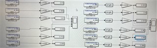
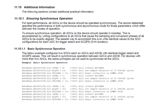
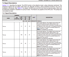
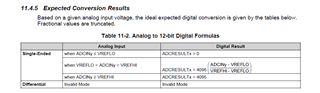
I am reading 12 voltage values using HIL setup, where 3 ADC with 4 channels are used (total 12), each ADC (A,B,C) are configured with different SOC (SOC0,SOC1,SOC2,SOC3) to read voltage values, but the problem is different offset values of each channel. The screenshot shows 12 reading with input voltage 2 volts where the ADC reads 2.30 to 2.41 volts and its changing every 1e-3 as I read every 1e-3 time. and also if I change the value from 2 volts to 2.5 or 3 volt then the offset is different. How to adjust this ADC offset? 

  • Hi, 

    Just to confirm my understanding, you would like to change your ADC offset because your ADC samples are not accurate? This is possible, but the typical offset error of the ADCs on the F28379D device is much lower than 300 mV. What are you using as the reference voltage for the ADCs? Also, are you triggering the ADCs synchronously as described in this section of the TRM? 

    Best Regards,

    Ben Collier

  • Thank you for your response. I am using MATLAB Simulink to code microcontroller, I am not using CCS. MATLAB generate code itself, as I am not very much familiar with the code. The code generated by the MATLAB shows all ADC (A,B,C) have same trigger and ACQPS value, only channel selection and SOC value are different. 

    what is reference voltage for ADC? I am just reading 12 external signal each have voltage range from 2.5v to 3.3v.

    void config_ADCA_SOC0()
    {
      EALLOW;
      AdcaRegs.ADCSOC0CTL.bit.CHSEL = 2;   /* Set SOC0 channel select to ADCIN2*/
      AdcaRegs.ADCSOC0CTL.bit.TRIGSEL = 1;
      AdcaRegs.ADCSOC0CTL.bit.ACQPS = 14.0;
                                   /* Set SOC0 S/H Window to 15.0 ADC Clock Cycles*/
      AdcaRegs.ADCINTSOCSEL1.bit.SOC0 = 0;
                                       /* SOCx No ADCINT Interrupt Trigger Select.*/
      AdcaRegs.ADCOFFTRIM.bit.OFFTRIM = AdcaRegs.ADCOFFTRIM.bit.OFFTRIM;/* Set Offset Error Correctino Value*/
      AdcaRegs.ADCCTL1.bit.INTPULSEPOS = 1;
                                    /* Late interrupt pulse trips AdcResults latch*/
      AdcaRegs.ADCSOCPRICTL.bit.SOCPRIORITY = 0;/* All in round robin mode SOC Priority*/
      EDIS;
    }

    void config_ADCA_SOC1()
    {
      EALLOW;
      AdcaRegs.ADCSOC1CTL.bit.CHSEL = 3;   /* Set SOC1 channel select to ADCIN3*/
      AdcaRegs.ADCSOC1CTL.bit.TRIGSEL = 1;
      AdcaRegs.ADCSOC1CTL.bit.ACQPS = 14.0;
                                   /* Set SOC1 S/H Window to 15.0 ADC Clock Cycles*/
      AdcaRegs.ADCINTSOCSEL1.bit.SOC1 = 0;
                                       /* SOCx No ADCINT Interrupt Trigger Select.*/
      AdcaRegs.ADCOFFTRIM.bit.OFFTRIM = AdcaRegs.ADCOFFTRIM.bit.OFFTRIM;/* Set Offset Error Correctino Value*/
      AdcaRegs.ADCCTL1.bit.INTPULSEPOS = 1;
                                    /* Late interrupt pulse trips AdcResults latch*/
      AdcaRegs.ADCSOCPRICTL.bit.SOCPRIORITY = 0;/* All in round robin mode SOC Priority*/
      EDIS;
    }

    void config_ADCA_SOC2()
    {
      EALLOW;
      AdcaRegs.ADCSOC2CTL.bit.CHSEL = 4;   /* Set SOC2 channel select to ADCIN4*/
      AdcaRegs.ADCSOC2CTL.bit.TRIGSEL = 1;
      AdcaRegs.ADCSOC2CTL.bit.ACQPS = 14.0;
                                   /* Set SOC2 S/H Window to 15.0 ADC Clock Cycles*/
      AdcaRegs.ADCINTSOCSEL1.bit.SOC2 = 0;
                                       /* SOCx No ADCINT Interrupt Trigger Select.*/
      AdcaRegs.ADCOFFTRIM.bit.OFFTRIM = AdcaRegs.ADCOFFTRIM.bit.OFFTRIM;/* Set Offset Error Correctino Value*/
      AdcaRegs.ADCCTL1.bit.INTPULSEPOS = 1;
                                    /* Late interrupt pulse trips AdcResults latch*/
      AdcaRegs.ADCSOCPRICTL.bit.SOCPRIORITY = 0;/* All in round robin mode SOC Priority*/
      EDIS;
    }

    void config_ADCA_SOC3()
    {
      EALLOW;
      AdcaRegs.ADCSOC3CTL.bit.CHSEL = 5;   /* Set SOC3 channel select to ADCIN5*/
      AdcaRegs.ADCSOC3CTL.bit.TRIGSEL = 1;
      AdcaRegs.ADCSOC3CTL.bit.ACQPS = 14.0;
                                   /* Set SOC3 S/H Window to 15.0 ADC Clock Cycles*/
      AdcaRegs.ADCINTSOCSEL1.bit.SOC3 = 0;
                                       /* SOCx No ADCINT Interrupt Trigger Select.*/
      AdcaRegs.ADCOFFTRIM.bit.OFFTRIM = AdcaRegs.ADCOFFTRIM.bit.OFFTRIM;/* Set Offset Error Correctino Value*/
      AdcaRegs.ADCCTL1.bit.INTPULSEPOS = 1;
                                    /* Late interrupt pulse trips AdcResults latch*/
      AdcaRegs.ADCSOCPRICTL.bit.SOCPRIORITY = 0;/* All in round robin mode SOC Priority*/
      EDIS;
    }

    void config_ADCB_SOC0()
    {
      EALLOW;
      AdcbRegs.ADCSOC0CTL.bit.CHSEL = 2;   /* Set SOC0 channel select to ADCIN2*/
      AdcbRegs.ADCSOC0CTL.bit.TRIGSEL = 1;
      AdcbRegs.ADCSOC0CTL.bit.ACQPS = 14.0;
                                   /* Set SOC0 S/H Window to 15.0 ADC Clock Cycles*/
      AdcbRegs.ADCINTSOCSEL1.bit.SOC0 = 0;
                                       /* SOCx No ADCINT Interrupt Trigger Select.*/
      AdcbRegs.ADCOFFTRIM.bit.OFFTRIM = AdcbRegs.ADCOFFTRIM.bit.OFFTRIM;/* Set Offset Error Correctino Value*/
      AdcbRegs.ADCCTL1.bit.INTPULSEPOS = 1;
                                    /* Late interrupt pulse trips AdcResults latch*/
      AdcbRegs.ADCSOCPRICTL.bit.SOCPRIORITY = 0;/* All in round robin mode SOC Priority*/
      EDIS;
    }

    void config_ADCB_SOC1()
    {
      EALLOW;
      AdcbRegs.ADCSOC1CTL.bit.CHSEL = 3;   /* Set SOC1 channel select to ADCIN3*/
      AdcbRegs.ADCSOC1CTL.bit.TRIGSEL = 1;
      AdcbRegs.ADCSOC1CTL.bit.ACQPS = 14.0;
                                   /* Set SOC1 S/H Window to 15.0 ADC Clock Cycles*/
      AdcbRegs.ADCINTSOCSEL1.bit.SOC1 = 0;
                                       /* SOCx No ADCINT Interrupt Trigger Select.*/
      AdcbRegs.ADCOFFTRIM.bit.OFFTRIM = AdcbRegs.ADCOFFTRIM.bit.OFFTRIM;/* Set Offset Error Correctino Value*/
      AdcbRegs.ADCCTL1.bit.INTPULSEPOS = 1;
                                    /* Late interrupt pulse trips AdcResults latch*/
      AdcbRegs.ADCSOCPRICTL.bit.SOCPRIORITY = 0;/* All in round robin mode SOC Priority*/
      EDIS;
    }

    void config_ADCB_SOC2()
    {
      EALLOW;
      AdcbRegs.ADCSOC2CTL.bit.CHSEL = 4;   /* Set SOC2 channel select to ADCIN4*/
      AdcbRegs.ADCSOC2CTL.bit.TRIGSEL = 1;
      AdcbRegs.ADCSOC2CTL.bit.ACQPS = 14.0;
                                   /* Set SOC2 S/H Window to 15.0 ADC Clock Cycles*/
      AdcbRegs.ADCINTSOCSEL1.bit.SOC2 = 0;
                                       /* SOCx No ADCINT Interrupt Trigger Select.*/
      AdcbRegs.ADCOFFTRIM.bit.OFFTRIM = AdcbRegs.ADCOFFTRIM.bit.OFFTRIM;/* Set Offset Error Correctino Value*/
      AdcbRegs.ADCCTL1.bit.INTPULSEPOS = 1;
                                    /* Late interrupt pulse trips AdcResults latch*/
      AdcbRegs.ADCSOCPRICTL.bit.SOCPRIORITY = 0;/* All in round robin mode SOC Priority*/
      EDIS;
    }

    void config_ADCB_SOC3()
    {
      EALLOW;
      AdcbRegs.ADCSOC3CTL.bit.CHSEL = 5;   /* Set SOC3 channel select to ADCIN5*/
      AdcbRegs.ADCSOC3CTL.bit.TRIGSEL = 1;
      AdcbRegs.ADCSOC3CTL.bit.ACQPS = 14.0;
                                   /* Set SOC3 S/H Window to 15.0 ADC Clock Cycles*/
      AdcbRegs.ADCINTSOCSEL1.bit.SOC3 = 0;
                                       /* SOCx No ADCINT Interrupt Trigger Select.*/
      AdcbRegs.ADCOFFTRIM.bit.OFFTRIM = AdcbRegs.ADCOFFTRIM.bit.OFFTRIM;/* Set Offset Error Correctino Value*/
      AdcbRegs.ADCCTL1.bit.INTPULSEPOS = 1;
                                    /* Late interrupt pulse trips AdcResults latch*/
      AdcbRegs.ADCSOCPRICTL.bit.SOCPRIORITY = 0;/* All in round robin mode SOC Priority*/
      EDIS;
    }

    void config_ADCC_SOC0()
    {
      EALLOW;
      AdccRegs.ADCSOC0CTL.bit.CHSEL = 2;   /* Set SOC0 channel select to ADCIN2*/
      AdccRegs.ADCSOC0CTL.bit.TRIGSEL = 1;
      AdccRegs.ADCSOC0CTL.bit.ACQPS = 14.0;
                                   /* Set SOC0 S/H Window to 15.0 ADC Clock Cycles*/
      AdccRegs.ADCINTSOCSEL1.bit.SOC0 = 0;
                                       /* SOCx No ADCINT Interrupt Trigger Select.*/
      AdccRegs.ADCOFFTRIM.bit.OFFTRIM = AdccRegs.ADCOFFTRIM.bit.OFFTRIM;/* Set Offset Error Correctino Value*/
      AdccRegs.ADCCTL1.bit.INTPULSEPOS = 1;
                                    /* Late interrupt pulse trips AdcResults latch*/
      AdccRegs.ADCSOCPRICTL.bit.SOCPRIORITY = 0;/* All in round robin mode SOC Priority*/
      EDIS;
    }

    void config_ADCC_SOC1()
    {
      EALLOW;
      AdccRegs.ADCSOC1CTL.bit.CHSEL = 3;   /* Set SOC1 channel select to ADCIN3*/
      AdccRegs.ADCSOC1CTL.bit.TRIGSEL = 1;
      AdccRegs.ADCSOC1CTL.bit.ACQPS = 14.0;
                                   /* Set SOC1 S/H Window to 15.0 ADC Clock Cycles*/
      AdccRegs.ADCINTSOCSEL1.bit.SOC1 = 0;
                                       /* SOCx No ADCINT Interrupt Trigger Select.*/
      AdccRegs.ADCOFFTRIM.bit.OFFTRIM = AdccRegs.ADCOFFTRIM.bit.OFFTRIM;/* Set Offset Error Correctino Value*/
      AdccRegs.ADCCTL1.bit.INTPULSEPOS = 1;
                                    /* Late interrupt pulse trips AdcResults latch*/
      AdccRegs.ADCSOCPRICTL.bit.SOCPRIORITY = 0;/* All in round robin mode SOC Priority*/
      EDIS;
    }

    void config_ADCC_SOC2()
    {
      EALLOW;
      AdccRegs.ADCSOC2CTL.bit.CHSEL = 4;   /* Set SOC2 channel select to ADCIN4*/
      AdccRegs.ADCSOC2CTL.bit.TRIGSEL = 1;
      AdccRegs.ADCSOC2CTL.bit.ACQPS = 14.0;
                                   /* Set SOC2 S/H Window to 15.0 ADC Clock Cycles*/
      AdccRegs.ADCINTSOCSEL1.bit.SOC2 = 0;
                                       /* SOCx No ADCINT Interrupt Trigger Select.*/
      AdccRegs.ADCOFFTRIM.bit.OFFTRIM = AdccRegs.ADCOFFTRIM.bit.OFFTRIM;/* Set Offset Error Correctino Value*/
      AdccRegs.ADCCTL1.bit.INTPULSEPOS = 1;
                                    /* Late interrupt pulse trips AdcResults latch*/
      AdccRegs.ADCSOCPRICTL.bit.SOCPRIORITY = 0;/* All in round robin mode SOC Priority*/
      EDIS;
    }

    void config_ADCC_SOC3()
    {
      EALLOW;
      AdccRegs.ADCSOC3CTL.bit.CHSEL = 5;   /* Set SOC3 channel select to ADCIN5*/
      AdccRegs.ADCSOC3CTL.bit.TRIGSEL = 1;
      AdccRegs.ADCSOC3CTL.bit.ACQPS = 14.0;
                                   /* Set SOC3 S/H Window to 15.0 ADC Clock Cycles*/
      AdccRegs.ADCINTSOCSEL1.bit.SOC3 = 0;
                                       /* SOCx No ADCINT Interrupt Trigger Select.*/
      AdccRegs.ADCOFFTRIM.bit.OFFTRIM = AdccRegs.ADCOFFTRIM.bit.OFFTRIM;/* Set Offset Error Correctino Value*/
      AdccRegs.ADCCTL1.bit.INTPULSEPOS = 1;
                                    /* Late interrupt pulse trips AdcResults latch*/
      AdccRegs.ADCSOCPRICTL.bit.SOCPRIORITY = 0;/* All in round robin mode SOC Priority*/
      EDIS;
    }

  • Hi,

    Thank you for confirming that you are triggering the ADCs synchronously. Are you using a TI board or a custom board? The reference voltage for the ADCs is provided to these pins on the device (see below datasheet screenshot). There are also VREFLO pins, which are typically tied to ground. 

    It is important to be aware of what voltage reference you are using, since the meaning of output code of the ADC is determined by the reference voltage, as shown in the TRM screenshot below.   

    Best Regards,

    Ben Collier

  • I am using  TI board LaunchXL-F28379D. Which have voltage range (0-3.3 volts), directly connected to PC using USB port that provides 5 volts, which is further divided internally into 3.3 volts as required. As VREFLO< ADCINy < VREFHI , that's why  ADC block output is multiplied by gain (3.3/4095) to get real voltage value. 

    My main issue is ADC offset , I read fix voltage 1 or 2 volt from TI board pins but the MATLAB Simulink shows random offset? is this an issue of USB cable that connects TI board with MATLAB? 

  • what is reference voltage for ADC?

    It's 3.0V. If you look at the schematic of the LAUNCHXL-F28379D, there's a voltage reference IC REF5030IDGKT.

    I would suggest to change all the gain blocks in your model to 3.0/4095.

  • Kier,

    Thank you for your input. I agree, Adnan needs to change the gain to (3.0/4095).

    Adnan,

    Please let me know if your problem persists after making this change.

    Best Regards,

    Ben Collier

  • Thanks. I changed my Voltage ref to 3 volt which reduce the offset error. And I find out  the offset error was not due to ADC but it was because of input signal , which variation of around 50mv. I may have to use filters to reduce signal noise. 

  • Ok,

    I am glad that you seem to have found a solution to your problem. Please re-open this thread if you have further issues with this, or start a new thread if you have a new issue.

    Best Regards,

    Ben Collier