This thread has been locked.

If you have a related question, please click the "Ask a related question" button in the top right corner. The newly created question will be automatically linked to this question.

TMS320F280048-Q1: PCMC unexpected DC current

Part Number: TMS320F280048-Q1
Other Parts Discussed in Thread: PMP23126

Hi,

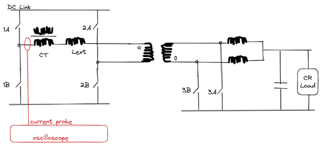
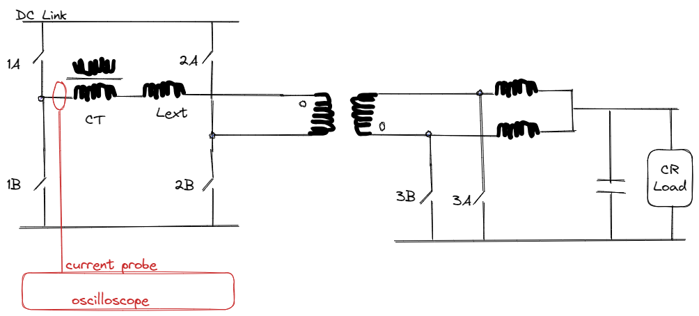
I'm testing my open loop PCMC controlled PSFB-CDR board at laboratory. It is TR-Lag drive topology. I showed below my driving scheme.

I just provide a Max value to CMPSS and change increase the input voltage. Load is bidirectional load and can take - currents.
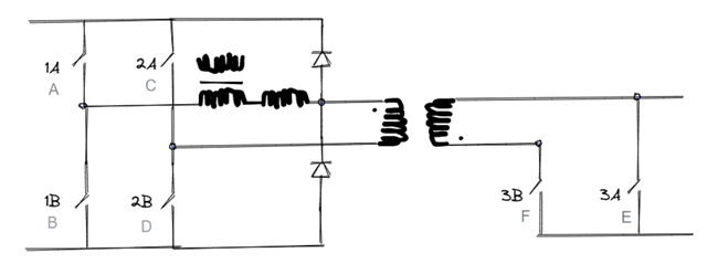
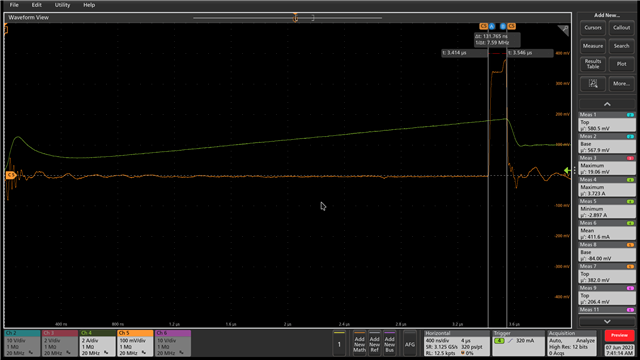
During tests, I got following waveforms; This case occurs during maximum duty cycle(peak not reached) to limiting the peak current boundary(peak current limits duty).
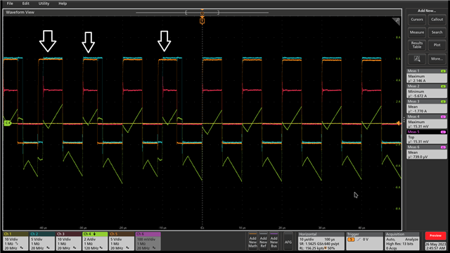
Blue is VGS,2B - Orange is VGS,1A - Red VDS,3B - Green is currnet on shim inductor.

In test condition, Vin and Vout is at CV mode and my PSFB board limits input current via PCMC strategy.

The mismatched duty cycle time cause transformer current to have a minus mean current, which satures transformer.

Can you help on it?

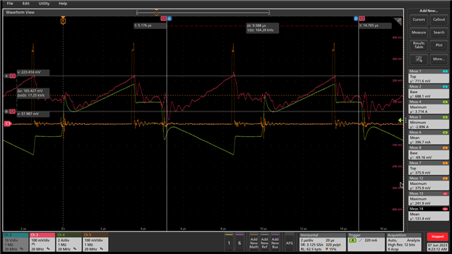
This the normal duty control phase waveform, which is good but I also have negative DC current at sensed line.

Can you help on the issues?

  • Hi Gokhan,

    Our Subject Matter Expert is out of office. Please expect the response by Tuesday. Thank you for your patience.

    Regards
    Srikanth

  • Hello Gokhan,

    I'm reviewing your query. If I understand correctly, you are observing that 1A is tripping before the peak current value is reached, which is not yielding the correct duty cycle, is this right? is it possible to add the CMPSS trip output here as well? 

  • Hi Gus,

    In above case, Yes. I can test whatever you need!!!

    I prepared a new test setup, and I can test what if you need. 

    Test condition for below waveform: 

    - I updated software and now PWM2 terminated power transfer interval. It is TR-LEAD Topology.

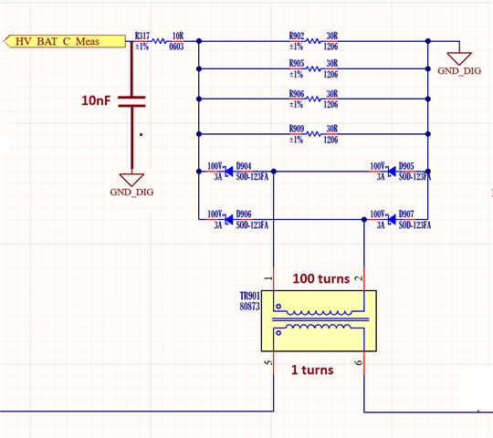
    - I removed clamp diodes and therefore my current sense transformer is inline with my transformer.

    -CMPC is used to generate SYNCPER signal.

    ePWM1 is loaded as Period, ePWM2 is Period -1, and ePWM8 is Period -1. (According to PMP23126 reference software)

     -I filter out the CMPSS output, CMPSS_TRIP_FILTER. But it doesn't make difference using instead of CMPSS_TRIP_ASYNC_COMP.

    - I provide same deadtime to all PWM modules! It is 120nsec!

    I obtained following waveforms. I signal out the OUTPUTXBAR 5 for CMPSS5OUT!

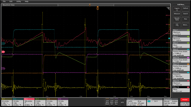
    I got following waveforms! Vin=150V, Vout=6V, Iout=24A Load is CR electronic load. CR=0.25ohm (%5 of rated output power)

                                               CMPSS Ramp Max Value = 6000, and Slope = 5 (as digital)

                                                Lmag=290uH, Lout=2.5uH, CT = 1 : 100 and Burden resistor is 7.5ohm

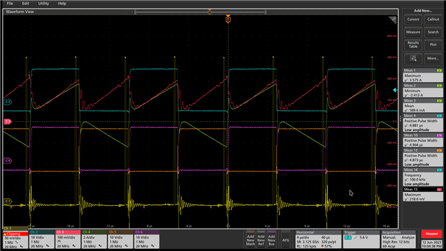
    Orange CMPSS Output, Green Current on CurrentSenseTransformer 

    As you can see from measurement table I have DC mean current!

    I'm zooming them.

    When I changed the deadtime of PWM2 from 120nsec to 200nsec or higher, my DC mean current decreases!!! I use UCC21530B as driver!

    I need your help. Thank you in advance.

  • Gokhan,

    Let me review these with some folks here and get back to you. 

    From these new plots it doesn't look like you are getting the CMPSS trip below the peak current, correct? Is it the case that the DC current is blocked from the input to the CMPSS? 

  • Gus,

    Yes, at new plots CMPSS trips and provides duty cycle control. But it isn't as good as I expected. It is steady state condition!

    As a general explanation, I have had two main problem, one of them is the transition state (during increasing input voltage) that I showed at my first post. It causes transformer to have DC current. The other problem is the mismatch at peak currents which also causes DC current on transformer during steady state condition, where input voltage is constant. I also showed it at my first post.

    At new plots, it is very close to my first post in steady state test condition. However, now, I changed leading leg from 1 to 2 (same as PMP23126). I ignored that transition condition (during input voltage increase) that causes CMPSS trips wrong. First of all, I focused on solving steady state condition. We shouldn't have any DC current on transformer.

    I also added voltage on output of current sense transformer on burden resistor (ADC voltage). Condition is same as above.

    Thank you in advance.

  • From these new plots it doesn't look like you are getting the CMPSS trip below the peak current, correct? Is it the case that the DC current is blocked from the input to the CMPSS?
    Yes, at new plots CMPSS trips and provides duty cycle control. But it isn't as good as I expected. It is steady state condition!

    Not sure if my point came across. What I mean is that if you look at the CMPSS trip output vs the value of the current, the CMPSS appears to be always tripping at the correct current minus DC offset. if the CMPSS was truly seeing the current with DC offset, then we would see uneven periods between CMPSS trip outputs. Does that make sense?

    I discussed with a few folks here. Consensus is that this DC current offset should not happen when using PCMC. We have no explanation for this. One possibility is measurement error. Could you describe how this measurement is being taken? Are you confident that measurement probe/setup itself is not introducing this offset? Another thing you could is to measure/plot the voltage input the CMPSS at the pin (or as close to) of the MCU. Having the phase-shifted PWM cycles on the same plot would help too.

  • Hi Gus, thank you for your effort. 

    Not sure if my point came across. What I mean is that if you look at the CMPSS trip output vs the value of the current, the CMPSS appears to be always tripping at the correct current minus DC offset. if the CMPSS was truly seeing the current with DC offset, then we would see uneven periods between CMPSS trip outputs. Does that make sense?

    Hmm, you say that there may be unreal DC current at the oscilloscope screen. I need to check the test setup. I didn't block any DC current through on my setup. However, CMPSS may trip at wrong positions and cause DC current. The mismatched time coordination for positive and negative half cycle, it may react like that.

    I drawed my measurement setup.

    I increase input voltage from 0V -------> 150V, I used CR mode of electronic load. While increasing input voltage from 0V to 150V, duty starts from %50 (which is max for PSFB) than decreases to %36.5 .However, during duty transition I have unstable waveforms as my first post. Maybe, it causes a DC current but it cannot be reset through switching interval. Maybe, there isn't enough DCR at transformer.

    Another option; I provide same deadband for both legs. However, T1 event causes 40nsec delay its inside. When I changed the deadtime of PWM2 from 120nsec to 200nsec or higher, my DC mean current decreases!!! I use UCC21530B as driver!

    Maybe slope isn't enough for correct operation. 

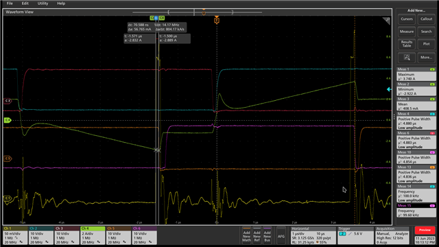
    I posted waveforms as below. All is same test condition I used cursors. I added pulse width for PWMs...

    YELLOW CMPSS TripOut, BLUE 1AVGS, RED 1BVGS, GREEN Ishim, ORANGE  2AVGS, PURPLE 2BVGS

    It seems that CMPSS trip at -2.8A and +3.6A.

    I can capture more waveforms if required.

    Thanks in advance.

  • As a reminder, I just test inner loop. I used constant resistor of electronic load at above waveforms.

    In below waveforms, I tested CV of electronic load.

    When I increase load voltage, below waveform occured.

  • However, CMPSS may trip at wrong positions and cause DC current.

    That's fair. What we are saying is that at this point we don't know the root cause of the DC current.

    It seems that CMPSS trip at -2.8A and +3.6A.

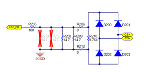
    The CMPSS has a single trip point. That trip point must lie between 0 and CMPSS VREF. On PMP23126 the primary current is rectified before it reaches the CMPSS. It still not clear from your plots what is the input to the CMPSS when current is -2.8A and 3.6A. 

  • Hi Gus,

    I showed my CT sensing network as below. I don't know why 9.76kohm is used at PMP23126, I don't have it.

    I can capture waveform at the ADCpin, which is also a CMPSS input. I can remove 1B Vgs signal and put the ADCInput signal if it is required?

    I also use analog to digital conversion at same pin, does it make problem?

  • I can capture waveform at the ADCpin, which is also a CMPSS input. I can remove 1B Vgs signal and put the ADCInput signal if it is required?

    Yes, that would be great.

    I also use analog to digital conversion at same pin, does it make problem?

    That should not be an issue.

  • Hi Gus,

    Q1) May the test condition wrong to test CMPSS? I use CR of electronic load and it is 0.25ohm. However, the output voltage varies depending on the current inside of CMPSS. That changes output voltage and duty.? Should I change the test condition, what would be the correct test condition to test PCMC loop?

    Q2) When peak current isn't reached, the duty becomes max and at that case I have unequal pulse width due to event triggering inside MCU. Does also make DC current and it might not to be zero before starting to real tripping. May it be the case?

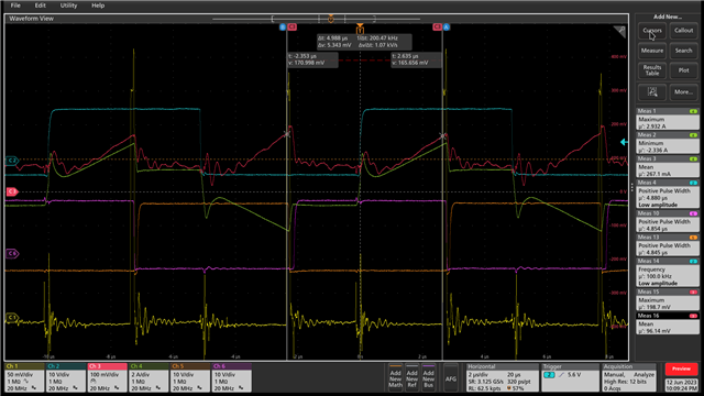
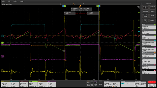
    I increase Vin from 0V to 150V. During ramping input voltage slowly I also take a measurement on 100V it is as below. The duty starts from max here CMPSS trip cannot react to duty.

    YELLOW CMPSS TripOut, BLUE 1AVGS, RED 1BVGS, GREEN Ishim, ORANGE  2AVGS, PURPLE 2BVGS

    #Waveform1 Vin=103V, Vout=5.71V, Iout = 22A, REF_CMPSS_PEAK= 6000, PSFB_SLOPE_INITIAL = 5

    #Waveform2 Vin=150V, Vout=6.1V, Iout = 24.38A, REF_CMPSS_PEAK= 6000, PSFB_SLOPE_INITIAL = 5

    #Waveform3 Vin=150V, Vout=6.1V, Iout = 24.38A, REF_CMPSS_PEAK= 6000, PSFB_SLOPE_INITIAL = 10

    In my test condition slope compensation limits peak current, because when I change the slope to 0, current cannot reach the RAMPMAX set value. I increase my electronic load power rating and maybe test it later.

    Thanks in advance.

  • Q1) May the test condition wrong to test CMPSS? I use CR of electronic load and it is 0.25ohm. However, the output voltage varies depending on the current inside of CMPSS. That changes output voltage and duty.? Should I change the test condition, what would be the correct test condition to test PCMC loop?

    For open loop, I would also use CR mode. The test steps are documented the PMP23126 user guide.

    Q2) When peak current isn't reached, the duty becomes max and at that case I have unequal pulse width due to event triggering inside MCU. Does also make DC current and it might not to be zero before starting to real tripping. May it be the case?

    Have you tried setting a lower peak current?

    Note: I will be OOO for next three days.