


Modification of the ADC chapter routines: adc_ex6_soc_continuous_dma.c,
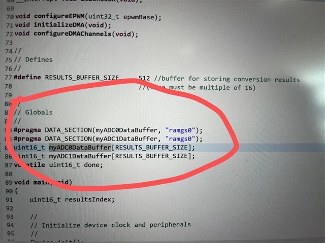
The ADCA conversion result is transferred to myADC0Buffer via DMA, currently modifying the FSI routines
This should specify the array of data to be transferred

This one routine says it is writing to the buffer to be transferred.
So if I change this txBufData directly to myADC0Buffer, will I be able to transfer the data collected by the ADC via FSI?
Another question is that this course is supposed to be about an 80 pin chip, I am using a 48 pin one, do I need to make any changes?

