Part Number: TMS320F28335
Hi Team,
The voltage sampling is not correct once the inverter sends a wave, the voltage sampling waveform is abnormal.
actual waveform:

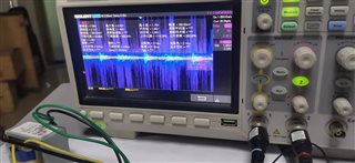
Schematic diagram of voltage sampling:


--
Thanks & Regards
Yale
This thread has been locked.
If you have a related question, please click the "Ask a related question" button in the top right corner. The newly created question will be automatically linked to this question.
Part Number: TMS320F28335
Hi Team,
The voltage sampling is not correct once the inverter sends a wave, the voltage sampling waveform is abnormal.
actual waveform:


Schematic diagram of voltage sampling:


--
Thanks & Regards
Yale
The subject matter expert is out of office, please expect a response by Wednesday.
Thanks.
Yale,
I think we are suspecting some noise caused by the inverter switching, is impacting the ADC sample. I'm assuming that the input to the C2000 ADC from the op-amp(and its output R/C) are located close to the C2000 MCU? If you could give some comment here it would be good to know.
We may have to accept that there will be noise due to the switching and move the ADC sample to accommodate. Have you tried to change the trigger for the ADC to happen before the switching action to see if that has a better noise profile? This would confirm that the switching action is what is causing the extra noise on the ADC sample.
Based on the ADC architecture I think we should be safe once the sample has completed and the ADC is converting; but if we are sampling the ADC input while the inverting is switching, we run the risk of sampling noise on top of the signal as you are seeing.
Best,
Matthew