This thread has been locked.

If you have a related question, please click the "Ask a related question" button in the top right corner. The newly created question will be automatically linked to this question.

TMS320F280039: ADC pin measurement daviation

Part Number: TMS320F280039
Other Parts Discussed in Thread: C2000WARE, REF3430, OPA320, REF5030

Dear expert,

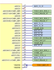
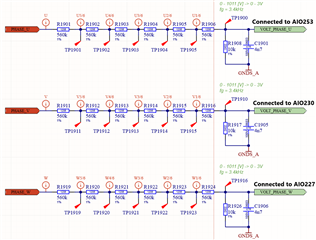
We are currently developing our application for TMS320F280039, and find out one of the ADC measurements is slightly higher from the expected value (AIO229), and it looks like pin is internally pulled-up. When we measure at the microcontroller pin.

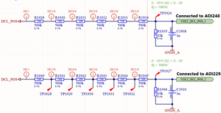
To debug are comparing two pins ( AIO229 and AIO248) which, after reviewing, apparently have the same configuration(no pull up, no inversion, sync), but  AIO229 shows this "offset".

Also, when measuring with a tester AIO229, the value is higher than expected, and after disconnecting AIO229  from the circuit, the measured value goes back to the "expected" voltage.

Do you know if there is any HW difference between these two pins that could provoke this? Or else, can you foresee any specific configuration that could lead to this behavior?

Regards,

Marc Ferrer

  • Hello Marc,

    Please kindly provide some more information to clarify:

    - Describe the circuit connected to the AIO pins (a schematic if possible);

    - How much offset are you seeing compared to the baseline? 

    Thanks,
    Ibukun

  • Hello Ibukun,

    I'm the hardware guy in this same project.

    The schematic looks as followed:

    The reference voltage (VREFHI) is 3V, the analog voltage (VDDA) is 3.3V.

    The following measurements show the error (voltage increase) on TP1927 (AOI248) as well as a ADC-Error on VOLT_DCL_POS_1 at 200V.

    UHV / V TP1924 / V TP1927 / V Reference value Tolerance AD-RAW
    VOLT_DCL _POS_1
    AD-RAW
    VOLT_DCL _POS_2
    0 0.001 0.000 0 0 - 6 19 0
    100 0.298 0.301 405 395 - 414 404 408
    200 0.594 0.632 810 797 - 822 823 870
    300 0.89 0.935 1215 1199 - 1230 1225 1280
    400 1.188 1.235 1620 1601 - 1638 1627 1685
    500 1.484 1.533 2025 2003 - 2046 2028 2089
    600 1.781 1.830 2430 2406 - 2454 2431 2492
    700 2.075 2.125 2835 2808 - 2862 2831 2892
    800 2.376 2.424 3240 3210 - 3270 3233 3294
    900 2.676 2.726 3645 3612 - 3678 3637 3697
    1000 2.970 3.018 4050 4014 - 4086 4037 4095

    As you can see, the voltage is higher at TP1927 as the voltage dividor would allow.

    I then also repeated the measurement up to 300V with the microcontroller in reset (Pin nXRS connected to GND) and the voltage rise on AOI229 got smaller.

    UHV / V TP1924 / V TP1927 / V Reference value in V
    0 0 -0.001 0.000
    100 0.298 0.3 0.297
    200 0.593 0.614 0.593
    300 0.89 0.915 0.890

    I then disconnected the Signal "VOLT_DCL_POS_2" from the AOI229 Pin (Pin 18) and repeated the measurement again up to 300V. (Pin nXRS still connected to GND) The error on TP1927 is now gone.

    UHV / V TP1924 / V TP1927 / V Reference value in V
    0 0 0 0.000
    100 0.297 0.297 0.297
    200 0.594 0.594 0.593
    300 0.89 0.89 0.890
  • During the same time we applied the same voltage UHV to the following 3 circuits. And the behaved as expected:

    The ADC Channels chosen are the following (correct me Marc if I'm wrong)

    VOLT_DCL_POS_1 AIO248 C1
    VOLT_DCL_POS_2 AIO229 A3
    VOLT_PHASE_U AIO253 C11
    VOLT_PHASE_V AIO230 B1
    VOLT_PHASE_W AIO227 A9
  • Hello Cedric and Marc,

    This may be a long shot, but have you tried explicitly disabling all pull-ups on the AIO pins? Basically, write 0xFFFFFFFF to the GPHPUD register. It does sound like an internal pull-up is affecting it, although it really ought to have been disabled by default.

    The offset does also seem to be fairly constant - in the range of 50-60 LSBs or so. One mitigation option here might be to use the ADC PPB offset calibration feature, which can automatically add an offset value from -512 to 511 to the ADC conversion result.

    Ibukun

  • Hello Ibukun,

    I can't find GPHPUD register on the code. I searched on the C2000ware with no success.  Also, Technical Reference Manual is only mentioning GPHPUD on the last revision of the document which is from 06/2023, so the one I was using until now is also not mapping this register. Do you think mismatch could be related to the issue?

    Moreover, we also tested by writing 0xFFFFFFFF to the register address where GPHPUD register should be, but the result was the same. 

    Thanks in advance,
    Marc

  • We did some more testing and I think we found the root cause for the problem.

    On one Channel, AIO226 we measure the DCL voltage in the range of 0-75 to have a better accuracy. Since the DCL voltage can go up to 1000V we added a clamping diode, but it seems, that the clamping is not strong enougth.

    When the voltage on TP1935 exceeds the 3V reference we start to see an influence on some ADC-channels but not on all.

    Influence at UHV = 100V compared to 0V  3.72V @ TP1936
     
    Pin YES/NO AIO-#
    14 NO AIO228
    15 YES AIO226
    16 YES AIO242
    17 YES AIO224
    18 YES AIO229
    19 NO AIO239
    20 NO AIO237
    21 YES AIO244
    22 NO AIO232
    23 NO AIO231
    24 NO VREFHI
    25 NO VREFHI
    26 NO VREFLO
    27 NO VREFLO
    28 YES AIO238
    29 NO AIO248
    30 YES AIO251
    31 YES AIO245
    32 YES AIO252
    33 NO VSSA
    34 YES VDDA
    35 YES AIO249
    36 YES AIO225
    37 YES AIO240
    38 YES AIO227
    39 YES AIO236
    40 NO AIO230
    41 NO AIO253
    42 YES AIO247

    Could you give us an overview over the internal clamping?

  • Cedric,

    That's good news to hear you were able to track this down. The clamping mechanism you have in the diagram above is actually the same mechanism used in the device at the input pin cell. These diodes are primarily intended for ESD protection but have the effect of sinking or sourcing current whenever the input voltage exceeds the operating range. The exact forward bias voltage for the diodes is not specified, however.

    In my testing, I have found that the clamping diode will sink current on the order of a few mA when it is turned on.

    Best regards,
    Ibukun

  • One point of clarification: the top diode is connected to the VDDA supply rail, which is nominally 3.3V (this is different from VREF which in your case is 3.0V).

    Best regards,
    Ibukun

  • Yes, we expected the clamping mechanism to be a diode to VDDA on every analog pin.

    Since we knew, that the voltage on TP1935 will exceed 3V and potentially go up to 40V we added the external claping diode and a 10k series resistor to limit the current into the pin to approx. 30uA.

    If (as expected) every ADC Pin has a seperate clamping diode towards VDDA we should protect the ADC Pin VOLT_DCL_POS_3 / AIO226 / Pin 15 effectively.

    What I now don't understand, is that we see an effect on other ADC Pins from this current.

    On VOLT_DCL_POS_3 / AIO226 / Pin 15 we measure 3.72V with UHV = 100V. This is below the max. Input voltage of 4.6V in the datasheet and as established above, the current is also limited to approx. 30uA.

    Are the ADC-Pins also grouped somehow besides the clamping diode on every Pin? They somehow need to be, in order to see the dsescribed effect of a voltage rise on other ADC-Pins but not all.

  • Ok, I am one step closer to the solution:

    I adjusted the clamping and measurement circuit of VOLT_DCL_POS_3 / AIO242 to limit the voltage below 3.3V

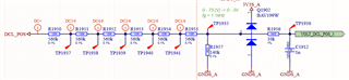
      Ra = 300e, Rb = 1k, R1957 = 121k
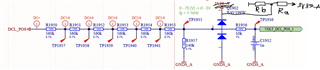
    Nevertheless I see a small deviation to the expected ADC result in the lower voltages.

    UHV / V TP1924 / V TP1927 / V Reference value in V Reference value Tolerance Design AD-RAW AD-RAW
    VOLT_DCL _POS_1 VOLT_DCL _POS_2
    0 0.000 0.000 0.000 0 0 - 6 17 0
    70 0.209 0.209 0.208 284 275 - 291 300 296
    100 0.298 0.298 0.297 405 395 - 414 421 417
    200 0.596 0.595 0.593 810 797 - 822 823 818
    300 0.892 0.893 0.890 1215 1199 - 1230 1225 1221
    400 1.190 1.189 1.187 1620 1601 - 1638 1626 1623
    500 1.490 1.489 1.484 2025 2003 - 2046 2028 2024
    600 1.783 1.783 1.780 2430 2406 - 2454 2431 2426
    700 2.079 2.078 2.077 2835 2808 - 2862 2832 2828
    800 2.381 2.381 2.374 3240 3210 - 3270 3233 3229
    900 2.672 2.673 2.671 3645 3612 - 3678 3636 3632
    1000 2.974 2.973 2.967 4050 4014 - 4086 4039 4035

    What I can say for sure is, that all voltages on all ADC Pins are below VDDA.

    But we use several AIO as digital inputs, that are usually always high and do not switch, except in the event of a mayor fault. (This is why I placed those digital input signals on the spare AOI pins.)

    Is it possible, that the nFLT and RDY signals that are all constantly 3.3V somehow influence the high impedance measurement of VOLT_DCL_POS_1 and VOLT_DCL_POS_2?

    If yes, what can be done about it?

    My guess comes from the fact, that both VOLT_DCL_POS_1 (Pin29) and VOLT_DCL_POS_2 (Pin18) have nFLT and RDY signals close by. The also high impedance measurements of VOLT_PHASE_U/V/W that are basically the same circuit show no inaccuracies and have no nFLT and RDY signals close by.

  • Ok, I now tried to test if there is a influence of the digital signals on the AOI pins to the ADC values, and there is not.

    I reduced the voltage on the RDY and nFLT signals to 3V. -> no Change on the AD-RAW values.

    I also applied 70V to UHV  and then changed to voltage individually to 0V on the other AOI inputs. This also did not change the AD-RAW values measured.

    Could you help us understand the ADC error we see on the Channels VOLT_DCL_POS_1 / AIO248 and VOLT_DCL_POS_2 / AIO229?

    Best regards,

    Cedric Gasser

  • Hello Cedric,

    I think the clamping issue has been resolved. What I see in your data now is a basic gain error problem, which would primarily be a characteristic of your voltage reference. The gain error is about 0.72%. In the chart below, the blue is the test point voltage and the orange is the ADC conversion, which is linear but has a slightly different slope (gain).

    Can you describe your voltage reference circuit? What components are you using?

    We might also want to confirm that you are using the ADC_setVref() function correctly to enable the external reference and load the trims correctly. If ADC_setVref() is not used, it is possible that the device will be incorrectly trimmed during ADC operation.

    Best regards,
    Ibukun

  • Hello Ibukun,

    I also think that the clamping issue is resolved. (At the very least I hope so :-) )

    We use the component "REF3430-Q1" as reference voltage in the following circuit:

    As for how we are using the reference function in the uC I have to refer to Marc.

    Best regards,
    Cedric

  • Hello Ibukun,

    I can confirm we are using ADC_setVref during initialization of the three ADC modules (as ADC_REFERENCE_EXTERNAL and ADC_REFERENCE_3_3V).Before that, we are also calling SysCtl_deviceCal. 

    Regards,

    Marc Ferrer

  • Hello Cedric,

    The 200nF cap on the Vref pin is too much. REF3430 is only rated for 10uF on the output, and this 12-bit ADC should be fine with 2.2-4.7uF for VREFHI cap.

    Ibukun

  • Hello Ibukun,

    I'm sorry, but I'm not sure if I understand your advice

    The only capacitance we have on VREFHI at the moment, are the 2x 100nF. One cap close to the reference and one cap close to the microcontroller. If I understand you correctly, this is not enougth. (and not too much)
    I assume I should replace the 100nF cap close to the microcontroller with a 2.2-4.7uF cap?

    Regards, Cedric

  • Hello Cedric,

    I'm saying 100nF is too much for the REF3430 to support. 2x100nF is even worse Slight smile

    The total load cap cannot exceed 10uF per the REF3430 data sheet.

    Best regards,
    Ibukun

  • But 100nF or 200nF are way less than 10uF

    100 nano farad < 10 micro farad

  • Apologies! My brain's a little scrambled this morning.

    Yes, 100nF is too little. Minimum should be 2.2uF. You can put one 2.2uF near the reference and another 2.2uF near the pin and that works.

  • Hello Ibukun,

    Unfortunately, the corrected capacitance of 2x 2,2uF did not solve our issue:

    The measurement from 0 to 300V still looks the same.

    UHV / V TP1924 / V TP1927 / V Reference value in V Reference value Tolerance Design AD-RAW AD-RAW
    VOLT_DCL _POS_1 VOLT_DCL _POS_2
    0 0.001 0.000 0.000 0 0 - 6 18 0
    70 0.209 0.209 0.208 284 275 - 291 300 296
    100 0.298 0.298 0.297 405 395 - 414 421 417
    200 0.594 0.594 0.593 810 797 - 822 823 819
    300 0.891 0.891 0.890 1215 1199 - 1230 1224 1220

    Any other suggestions?

  • The only other relevant thing I can think of now is the ACQPS setting. I believe your team has already worked through this previously, but maybe it should be revisited. Insufficient acquisition time in this case could manifest as a gain error problem (you can see the conversion-to-expected delta decrease as the input voltage increases/required S+H cap charge time is increasing).

    That, coupled with an offset error on VOLT_DCL_POS_1 (manifested as 18 LSBs at 0V) could explain the characteristic graph I posted above. If the offset cannot be eliminated on board, the ADC has a feature to automatically correct systematic offset errors using PPB offset calibration (PPBxOFFCAL register).

    Ibukun

  • Hello Ibukun,

    We tried increasing significantly the acquisition time and the results were the same.

    We did a second test by swapping SOC2 signals with SOC3 signals (VOLT_DCL_POS_1 and VOLT_DCL_POS_2 were converted from SOC3). Once we perform the swap, we see a difference in the results as follows:

    Original Code:

    UHV / V TP1924 / V TP1927 / V Reference value in V AD-RAW AD-RAW
    VOLT_DCL _POS_1 VOLT_DCL _POS_2
    0 0.001 0 0 18 0
    70 0.209 0.209 0.208 300 296

    Swap SOC2 signals with SOC3 signals:

    UHV / V TP1924 / V TP1927 / V Reference value in V AD-RAW AD-RAW
    VOLT_DCL _POS_1 VOLT_DCL _POS_2
    0 0.001 0 0 11 0
    70 0.209 0.209 0.208 294 281

    Do you think this could be an indication of memory cross-talk issues? Otherwise, would you have any other suggestion?

    Thanks in advance,

    Marc

  • Hello Marc,

    I will attempt to follow up on this topic on Monday. Crosstalk is a possibility.

    Ibukun

  • Hello Ibukun,

    In order to provide more information, under the assumption that we might be facing memory crosstalk, we've also tested by swapping SOC0  with SOC3 signals. (VOLT_DCL_POS_1 and VOLT_DCL_POS_2).

    We see that once we move VOLT_DCL_POS_1 and VOLT_DCL_POS_2 to SOC0, its value is lower (We think this result is compatible with memory crosstalk). We also see higher values on signals sampled on SOC3 (previous on SOC0), but the offset is not as high as the other signals, so we wonder if there are other variables to take into account.

    Hope this might help to have a better overview.

    Thanks in advance,

    Marc Ferrer

  • Marc,

    The most direct solution to memory crosstalk is to sample VREFLO in between conversions, obviously at the expense of potentially reduced overall throughput depending on your control loop frequency/budget.

    Beyond that, we have an application note that deals with this particular topic in depth: Methods for Mitigating ADC Memory Cross-Talk

    Ultimately this is an inherent issue with high impedance signal sources; it becomes a cost vs performance tradeoff.

    However, you can always auto-compensate for systematic offset IF you know that it is relatively static/not variable, by using the ADC PPB (offset calibration). A dynamic offset is much harder to deal with.

    Best regards,
    Ibukun

  • Dear Ibukun,

    We have tested the proposed strategy on " Methods for Mitigating ADC Memory Cross-Talk" (sampling vreflo).  The offset we are seeing is linearly increasing as the measured signal voltage increases (the assumption is that this is aligned with memory crosstalk issue), so my understanding is that we can't use ADC PPB in that case, am I right?

    Is there any other ADC config, like adjusting Acq window, that could mitigate that?

    Also, is there any way to double check what we are experiencing is in fact, memory crosstalk? 

    Thanks in advance,

    Marc Ferrer

  • Marc,

    This is what I indicated previously - linearly increasing error over the input voltage range is gain error. Normally this should be directly attributable to the voltage reference accuracy (you can verify this by scoping VREFHI during the conversion phase to see both the rest voltage and load regulation behavior is - does it dip a little during conversion?).

    Based on the data you supplied earlier, I had calculated a gain error of 0.72% which is much greater than the spec accuracy of the REF3430 (0.05%). Perhaps there are other (dynamic?) factors at play here. The ideal configuration for the voltage reference on a SAR ADC is to combine the series reference part (REF3430, REF5030) with a high-bandwidth op amp buffer such as OPA320.The inherent gain error of the ADC itself is less than 0.002% FSR, so any observed gain error is attributable to factors external to the device.

    The PPB only helps with base offset error, not gain error (note that you could have both). Any adjustment for gain error must be done in software.

    On the crosstalk question, a simple test would be to disable all other SOC/channel triggers and simply sample the signal being tested repeatedly. You should have a stable, repeatable conversion value. If the first one or two conversions are lower and the rest are higher, that suggests the ACQPS is not long enough (assuming you started from a zero sampling cap state). Now if the accuracy of the signal changes when other SOCs/channels are enabled and converting, then memory crosstalk is confirmed.

    Best regards,
    Ibukun