This thread has been locked.

If you have a related question, please click the "Ask a related question" button in the top right corner. The newly created question will be automatically linked to this question.

EPWM sync via FSI

Part Number: TMS320F280049C
Other Parts Discussed in Thread: LAUNCHXL-F280049C, TMS320F280039C

Hi C2000 experts,

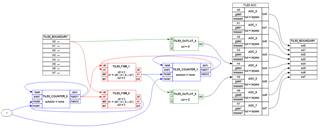
I want to synchronize ePWM modules on multiple devices via FSI in star topology. For this I played around with your example project "fsi_daisy_epwmsync_lead" on the LAUNCHXL-F280049C. I have a few questions about this.

For the sake of simplicity, I used the FSI loopback mode on a single F280049C controller. I configured the PWM slightly different and skipped the handshake initialization. I start a ping frame manually inside the debug session. If needed I can paste the code, but it should have no relation to my questions.

Here you can see a measurement:

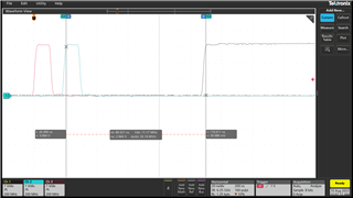
Ch1 (black): ePWM1A (set when TBCTR = 0, cleared when TBCTR = PRD)

Ch2 (blue):  EPWMSYNCIN (EPWMSYNCIN signal with delay from CLB, according to the example)

Ch3 (red): FSIRXA PING Packet Received / CLB_GLOBAL_IN_MUX_FSIRXA_PING_PACKET_RCVD (EPWMSYNCIN signal without delay, according to the example)

SYSCLK = EPWMCLK  = 100 MHz

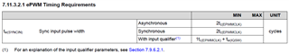
The pulse width of the "FSIRXA PING Packet Received" signal is only about one SYSCLK period. The CLB logic generates a delayed singal which is used as EXTSYNCIN1 in the ePWM. However, this signal is also only one SYSCLK period wide. In the data sheet SPRS945G of the controller, however, in section 7.11.3.2.1 a minimum pulse duration of two EPWMCLK cycles is required (asychronous). Since EPWMCLK is equal to SYSCLK, this time is violated. I have extended the pulse length up to 5 SYSCLK cycles by changing the clb configuration. But I found out that a longer pulse does not cause any change.

1) Is the synchronization of the example operated outside the specification, or is the value in the data sheet incorrect?

The cursors shows the latency between EPWMSYNCIN impulse and synchronization event. The delay is about 90 ns, which corresponds to 9 EPWMCLK cycles.

2) Is this delay specified anywhere in the TRM or in the data sheet?

3) Is this delay the same for all devices with type 4 ePWM units?

I found this in chapter 18.4.3.3. of the TRM SPRUI33F:

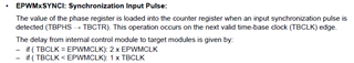
I assume that with internal module already an ePWM is meant and the delay of a chain, e.g. EXTSYNCIN1-> ePWM1 -> ePWM2 is described. Is this correct?

4) Is there any specification about the pulse length of the FSIRX pulses e.g. for FSIRXA PING Packet Received? I have not found anything in the TRM nor in the datasheet.

By measurements I found out that these pulse widths correspond to one SYSCLK period with type 0 FSI. With a FSI type 2, however, I could measure eight SYSCLK periods.

Thank you very much in advance.

Regards, Stefan

  • Hi Stefan,

    How are you going about bringing out the EPWMSYNCIN signal to a pin for probing?

    I'll need to check and get back to you on questions 1-3.

    4) Is there any specification about the pulse length of the FSIRX pulses e.g. for FSIRXA PING Packet Received? I have not found anything in the TRM nor in the datasheet.

    No we don't specify this internal signal.

    By measurements I found out that these pulse widths correspond to one SYSCLK period with type 0 FSI. With a FSI type 2, however, I could measure eight SYSCLK periods.

    What device did you use for the Type 2 test? The ePWM types and sync schemes may be different on these two devices. Also the internal connections used for the sync solution may be implemented differently.

    Best,

    Kevin

  • Hi Kevin,

    thank you very much for your reply.

    How are you going about bringing out the EPWMSYNCIN signal to a pin for probing?

    I used the structure from your document SPRACM3E and the related example fsi_daisy_epwmsync_node. In this structure/project, the CLB is used to generate a sync signal based on the delayed "FSIRXA PING Packet Received" signal. The delayed signal is passed to a GPIO for probing via an XBAR output and read back to the EXTSYNCHIN1 signal via the XBAR input.

    I was searching for another way to pass the "FSIRXA PING Packet Received" signal or its delayed signal directly to the EPWMxSYNCI, but did not find anything else. So I think I need to keep the bypass over the GPIO and XBARs.

    Here is my slightly modified code based on the fsi_daisy_epwmsync_node example:

    //#############################################################################
    //
    // FILE:   fsi_daisy_epwmsync_lead.c
    //
    // TITLE:  FSI daisy chain topology with ePWM synchronization,
    //         lead device example
    //
    //! fsi_daisy_epwmsync_lead is for the lead device in the daisy-chain
    //! loop, fsi_daisy_epwmsync_node for the other N-1 devices(N>=2).
    //!
    //! In a real scenario two separate devices may power up in arbitrary order and
    //! there is a need to establish a clean communication link which ensures that
    //! receiver side is flushed to properly interpret the start of a new valid
    //! frame.
    //!
    //! The lead device in the daisy chain topology initiates and drives the
    //! handshake sequence and subsequent data transmissions.
    //!
    //! After above synchronization steps, FSI Tx/Rx can be configured as per use
    //! case i.e. nWords, lane width, enabling events, etc and start the infinite
    //! transfers. More details on establishing the communication link can be found
    //! in the device TRM.
    //!
    //! For the ePWM SYNC use case, each lead and node device configures a 20 KHz,
    //! 50% duty cycle PWM signal once the handshake sequence is complete.
    //! The PWMs of all node devices in the chain are intended to be synchronized
    //! to the lead device's PWM using the FSI communication link alone.
    //!
    //! The lead device is configured to continuously trigger FSI ping frame
    //! transmissions on ePWM compare events. The event is configured using
    //! the ePWM compare value, EPWM_CMPC_VALUE, and
    //! the event prescale value, EPWM_SYNC_EVENT_COUNT.
    //!
    //! The CLB has been used to ensure EPWM signal synchronism among the devices.
    //! Input received by the CLB will be the FSI_RX_EVT_PING_FRAME signal.
    //! Once the input is received, CLB counter starts counting up from 0.
    //! When the count reaches "match1" value, a signal is generated which is used as
    //! the EXTSYNCIN1 signal for EPWM of the node device. The "match1" value
    //! acts as the EXTSYNCIN1 delay for the device. Last device in the link will
    //! need no delay and the first device in the link will have the maximum delay
    //! to ensure synchronism between devices.
    //!
    //! Also, when the input is received by CLB, it forwards FSI_RX_EVT_PING_FRAME
    //! signal to the next device in link without any delay.
    //!
    //! On receiving an FSI ping frame at the node, the EPWMs for multiple node
    //! devices can be synchronized with lead device by the user, by
    //! setting appropriate \b counter_match_value in the CLB configuration.
    //! \b counter_match_value can be set by using the "match1" value under
    //! counter0 tab in the syscfg file that is available with project.
    //! The details on the value which can be kept for
    //! \b counter_match_value to start the calibration for the PWM
    //! synchronization can be checked as shown below.
    //!
    //! For a setup of 'N' node devices, the \b counter_match_value for
    //! device1 will be 37*(N-1), device2 will have the value as 37*(N-2),
    //! similarly deviceN will have 1 to be fed as the "match1" value.
    //!
    //! It has to be noted that these values will vary depending on the user setup.
    //! The values provided can be taken as the reference to start the calibration.
    //! User also needs to verify the serial number of the device in the
    //! target configuration file provided with the project.
    //!
    //! User can edit some of configuration parameters as per use case, similar to
    //! other examples.
    //!
    //! \b nLanes - Choice to select single or double lane for frame transfers
    //! \b txPingFrameTag - Frame tag used for Ping transfers
    //! \b counter_match_value - "match1" value for CLB which generates delay
    //! \b epwm_cmpc_value_var - Used to align the EPWMSYNCIN signal
    //!
    //!\b External \b Connections \n
    //!  For the FSI daisy-chain topology external connections are required to
    //!  be made between the devices in the chain. Each devices FSI TX pins need to
    //!  be connected to the FSI RX pins of the next device in the chain (or ring).
    //!  See below for external connections to include and GPIOs used:
    //!
    //!  External Connections Required:
    //!     - FSIRX_CLK  to  FSITX_CLK
    //!     - FSIRX_RX0  to  FSITX_TX0
    //!     - FSIRX_RX1  to  FSITX_TX1 [Only needed when nLanes = 2_LANE]
    //!
    //!  ControlCard FSI Header GPIOs:
    //!     - GPIO_27  ->    FSITX_CLK
    //!     - GPIO_26  ->    FSITX_TX0
    //!     - GPIO_25  ->    FSITX_TX1
    //!     - GPIO_13  ->    FSIRX_CLK
    //!     - GPIO_12  ->    FSIRX_RX0
    //!     - GPIO_11  ->    FSIRX_RX1
    //!
    //!  LaunchPad FSI Header GPIOs:
    //!     - GPIO_7   ->    FSITX_CLK
    //!     - GPIO_6   ->    FSITX_TX0
    //!     - GPIO_25   ->    FSITX_TX1
    //!     - GPIO_33  ->    FSIRX_CLK
    //!     - GPIO_12  ->    FSIRX_RX0
    //!     - GPIO_2  ->    FSIRX_RX1
    //!
    //! \b Watch \b Variables \n
    //!  - \b error          Non zero for transmit/receive data mismatch
    //!  - \b FSIRxintCount  Number of Data frame received
    //!
    //! GPIO pins where output can be monitored:
    //!  - GPIO_0  for EPWM1A output
    //!  - GPIO_58 for EPWMSYNCIN signal without delay
    //!  - GPIO_3  for EPWMSYNCIN signal with delay from CLB
    //!  - LED1 and LED2 for handshake process
    //!
    //#############################################################################
    // $TI Release: $
    // $Release Date: $
    // $Copyright:
    // Copyright (C) 2022 Texas Instruments Incorporated - http://www.ti.com
    //
    // Redistribution and use in source and binary forms, with or without 
    // modification, are permitted provided that the following conditions 
    // are met:
    // 
    //   Redistributions of source code must retain the above copyright 
    //   notice, this list of conditions and the following disclaimer.
    // 
    //   Redistributions in binary form must reproduce the above copyright
    //   notice, this list of conditions and the following disclaimer in the 
    //   documentation and/or other materials provided with the   
    //   distribution.
    // 
    //   Neither the name of Texas Instruments Incorporated nor the names of
    //   its contributors may be used to endorse or promote products derived
    //   from this software without specific prior written permission.
    // 
    // THIS SOFTWARE IS PROVIDED BY THE COPYRIGHT HOLDERS AND CONTRIBUTORS 
    // "AS IS" AND ANY EXPRESS OR IMPLIED WARRANTIES, INCLUDING, BUT NOT 
    // LIMITED TO, THE IMPLIED WARRANTIES OF MERCHANTABILITY AND FITNESS FOR
    // A PARTICULAR PURPOSE ARE DISCLAIMED. IN NO EVENT SHALL THE COPYRIGHT 
    // OWNER OR CONTRIBUTORS BE LIABLE FOR ANY DIRECT, INDIRECT, INCIDENTAL, 
    // SPECIAL, EXEMPLARY, OR CONSEQUENTIAL DAMAGES (INCLUDING, BUT NOT 
    // LIMITED TO, PROCUREMENT OF SUBSTITUTE GOODS OR SERVICES; LOSS OF USE,
    // DATA, OR PROFITS; OR BUSINESS INTERRUPTION) HOWEVER CAUSED AND ON ANY
    // THEORY OF LIABILITY, WHETHER IN CONTRACT, STRICT LIABILITY, OR TORT 
    // (INCLUDING NEGLIGENCE OR OTHERWISE) ARISING IN ANY WAY OUT OF THE USE 
    // OF THIS SOFTWARE, EVEN IF ADVISED OF THE POSSIBILITY OF SUCH DAMAGE.
    // $
    //#############################################################################
    
    //
    // Included Files
    //
    #include "driverlib.h"
    #include "device.h"
    
    #define PRESCALER_VAL   FSI_PRESCALE_50MHZ
    
    //
    // Globals, User can modify these parameters as per usecase
    //
    
    //
    // Transfer can be happen over single or double lane
    //
    FSI_DataWidth nLanes = FSI_DATA_WIDTH_1_LANE;
    
    //
    // Frame tag used with Data/Ping transfers
    //
    FSI_FrameTag txPingFrameTag = FSI_FRAME_TAG0;
    
    //
    // Globals, these are not config parameters, user are not required to edit them
    //
    uint16_t txEventSts = 0, rxEventSts = 0;
    uint16_t *txBufAddr = 0, *rxBufAddr = 0;
    
    volatile uint32_t fsiTxInt1Received = 0, fsiTxInt2Received = 0;
    volatile uint32_t fsiRxInt1Received = 0, fsiRxInt2Received = 0;
    uint32_t txTimeOutCntr = 0x100000, rxTimeOutCntr = 0x100000;
    volatile uint32_t FSIRxintCount = 0;
    
    volatile uint16_t i = 0;
    
    uint32_t error = 0;
    
    //
    // Function Prototypes
    //
    static inline void compare16(uint16_t val1, uint16_t val2);
    void disableAllFSIInterrupts(void);
    void checkReceivedFrameTypeTag(FSI_FrameType type, FSI_FrameTag tag);
    void initFSI(void);
    void testGPIO(void);
    __interrupt void fsiTxInt1ISR(void);
    __interrupt void fsiTxInt2ISR(void);
    __interrupt void fsiRxInt1ISR(void);
    __interrupt void fsiRxInt2ISR(void);
    
    void handshake_node(void);
    
    void ConfigPWM();
    
    //
    // EPWM Configurations
    // 20kHz PWM
    //
    #define EPWM_TIMER_TBPRD  2499U
    #define EPWM_CMPA_VALUE   1249U
    #define EPWM_CMPB_VALUE   1249U
    
    //
    // User can choose any of 16 ePWM SOC event triggers
    //
    FSI_ExtFrameTriggerSrc ePWMTrigSel = FSI_EXT_TRIGSRC_EPWM1_SOCB;
    
    //
    // ePWM base addresses to operate on selected module and also Sysctl Clock to
    // enable/disable them.
    // Need to change base address as per ePWM trigger selection in \b ePWMTrigSel
    //
    uint32_t ePWMBaseAddr = EPWM1_BASE;
    SysCtl_PeripheralPCLOCKCR epwmSysCtlClock = SYSCTL_PERIPH_CLK_EPWM1;
    
    //
    //CLB includes
    //
    #include "clb_config.h"
    #include "clb.h"
    
    uint32_t counter_match_value = TILE1_COUNTER_0_MATCH1_VAL;
    
    //
    // Main
    //
    void main(void)
    {
        //
        // Initialize device clock and peripherals
        //
        Device_init();
    
        //
        // Disable pin locks and enable internal pullups.
        //
        Device_initGPIO();
        testGPIO();
    
        //
        // Initialize PIE and clear PIE registers. Disables CPU interrupts.
        //
        Interrupt_initModule();
    
        //
        // Initialize the PIE vector table with pointers to the shell Interrupt
        // Service Routines (ISR).
        //
        Interrupt_initVectorTable();
    
        //
        // Initialize basic settings for FSI
        //
        initFSI();
        FSI_enableRxInternalLoopback(FSIRXA_BASE);
    
        //
        // Interrupts that are used in this example are re-mapped to ISR functions
        // found within this file. Total 4; FSI Tx/Rx :: INT1/INT2
        //
        Interrupt_register(INT_FSITXA_INT1, &fsiTxInt1ISR);
        Interrupt_register(INT_FSITXA_INT2, &fsiTxInt2ISR);
        Interrupt_register(INT_FSIRXA_INT1, &fsiRxInt1ISR);
        Interrupt_register(INT_FSIRXA_INT2, &fsiRxInt2ISR);
    
        //
        // Enable FSI Tx/Rx interrupts
        //
        Interrupt_enable(INT_FSITXA_INT1);
        Interrupt_enable(INT_FSITXA_INT2);
        Interrupt_enable(INT_FSIRXA_INT1);
        Interrupt_enable(INT_FSIRXA_INT2);
    
        //
        // Enable Global Interrupt (INTM) and realtime interrupt (DBGM)
        //
        EINT;
        ERTM;
    
    
        //
        // Configure CLB
        //
        SysCtl_enablePeripheral(SYSCTL_PERIPH_CLK_CLB1);
    
        CLB_enableCLB(CLB1_BASE);
        initTILE1(CLB1_BASE);
    
        //
        // Select Global input instead of local input for all CLB IN
        //
        CLB_configLocalInputMux(CLB1_BASE, CLB_IN0, CLB_LOCAL_IN_MUX_GLOBAL_IN);
        CLB_configLocalInputMux(CLB1_BASE, CLB_IN1, CLB_LOCAL_IN_MUX_GLOBAL_IN);
        CLB_configLocalInputMux(CLB1_BASE, CLB_IN2, CLB_LOCAL_IN_MUX_GLOBAL_IN);
        CLB_configLocalInputMux(CLB1_BASE, CLB_IN3, CLB_LOCAL_IN_MUX_GLOBAL_IN);
        CLB_configLocalInputMux(CLB1_BASE, CLB_IN4, CLB_LOCAL_IN_MUX_GLOBAL_IN);
        CLB_configLocalInputMux(CLB1_BASE, CLB_IN5, CLB_LOCAL_IN_MUX_GLOBAL_IN);
        CLB_configLocalInputMux(CLB1_BASE, CLB_IN6, CLB_LOCAL_IN_MUX_GLOBAL_IN);
        CLB_configLocalInputMux(CLB1_BASE, CLB_IN7, CLB_LOCAL_IN_MUX_GLOBAL_IN);
    
    
        //
        // Select FSI_PING_PKT_RCVD for CLB1, IN0
        //
        CLB_configGlobalInputMux(CLB1_BASE, CLB_IN0, CLB_GLOBAL_IN_MUX_FSIRXA_PING_PACKET_RCVD);
    
        //
        // Unused Inputs below
        //
        CLB_configGlobalInputMux(CLB1_BASE, CLB_IN1, CLB_GLOBAL_IN_MUX_EPWM2A);
        CLB_configGlobalInputMux(CLB1_BASE, CLB_IN2, CLB_GLOBAL_IN_MUX_EPWM2A);
        CLB_configGlobalInputMux(CLB1_BASE, CLB_IN3, CLB_GLOBAL_IN_MUX_EPWM2A);
        CLB_configGlobalInputMux(CLB1_BASE, CLB_IN4, CLB_GLOBAL_IN_MUX_EPWM2A);
        CLB_configGlobalInputMux(CLB1_BASE, CLB_IN5, CLB_GLOBAL_IN_MUX_EPWM2A);
        CLB_configGlobalInputMux(CLB1_BASE, CLB_IN6, CLB_GLOBAL_IN_MUX_EPWM2A);
        CLB_configGlobalInputMux(CLB1_BASE, CLB_IN7, CLB_GLOBAL_IN_MUX_EPWM2A);
    
        //
        // Select External for CLB1, IN0
        //
        CLB_configGPInputMux(CLB1_BASE, CLB_IN0, CLB_GP_IN_MUX_EXTERNAL);
    
        //
        // Unused inputs to GP register
        //
        CLB_configGPInputMux(CLB1_BASE, CLB_IN1, CLB_GP_IN_MUX_GP_REG);
        CLB_configGPInputMux(CLB1_BASE, CLB_IN2, CLB_GP_IN_MUX_GP_REG);
        CLB_configGPInputMux(CLB1_BASE, CLB_IN3, CLB_GP_IN_MUX_GP_REG);
        CLB_configGPInputMux(CLB1_BASE, CLB_IN4, CLB_GP_IN_MUX_GP_REG);
        CLB_configGPInputMux(CLB1_BASE, CLB_IN5, CLB_GP_IN_MUX_GP_REG);
        CLB_configGPInputMux(CLB1_BASE, CLB_IN6, CLB_GP_IN_MUX_GP_REG);
        CLB_configGPInputMux(CLB1_BASE, CLB_IN7, CLB_GP_IN_MUX_GP_REG);
    
        CLB_setOutputMask(CLB1_BASE, CLB_OUTPUT_12 | CLB_OUTPUT_13, true);
    
        //
        // Configure the ePWM for 20kHz
        //
        ConfigPWM();
    
        //
        // EXTSYNCHIN1 configured to be routed from CLB compensated output
        // GPIO-3 -> INPUTXBAR.INPUT5 -> EXTSYNCHIN1
        //
        SysCtl_setSyncInputConfig(SYSCTL_SYNC_IN_EPWM1,
                                  SYSCTL_SYNC_IN_SRC_EXTSYNCIN1);
    
        //
        // Configure ePWM output signal
        //
        GPIO_setPinConfig(DEVICE_GPIO_CFG_EPWM1A);
    
        //
        // Enable peripheral clk for ePWM
        //
        SysCtl_enablePeripheral(epwmSysCtlClock);
    
        //
        // Start ePWM
        //
        EPWM_setEmulationMode(ePWMBaseAddr, EPWM_EMULATION_FREE_RUN);
        SysCtl_enablePeripheral(SYSCTL_PERIPH_CLK_TBCLKSYNC);
    
        //
        // GPIO for monitoring SYNCH
        //
        XBAR_setOutputMuxConfig(XBAR_OUTPUT7, XBAR_OUT_MUX01_CLB1_OUT4);
        XBAR_enableOutputMux(XBAR_OUTPUT7, XBAR_MUX01);
        GPIO_setPadConfig(11, GPIO_PIN_TYPE_STD);
        GPIO_setPinConfig(GPIO_11_OUTPUTXBAR7);
    
        //
        // GPIO for monitoring SYNCH with delay
        //
        XBAR_setOutputMuxConfig(XBAR_OUTPUT4, XBAR_OUT_MUX03_CLB1_OUT5);
        XBAR_enableOutputMux(XBAR_OUTPUT4, XBAR_MUX03);
        GPIO_setPadConfig(27, GPIO_PIN_TYPE_STD);
        GPIO_setPinConfig(GPIO_27_OUTPUTXBAR4);
    
        //
        // GPIO-3 is routed back to XBAR_INPUT-5 which is connected to EXTSYNCHIN1
        //
        XBAR_setInputPin(XBAR_INPUT5, 27);
    
        //
        // XBAR Config
        // CLB to PWM XBAR (CLB1_OUT4 to XBAR_TRIP4)
        // PWM XBAR to FSI has been hard coded at the start of this code.
        // For details on the connection, refer to Ext Frame Trigger Mux
        // section of the FSI chapter in the device TRM.
        //
        XBAR_setEPWMMuxConfig(XBAR_TRIP4, XBAR_EPWM_MUX01_CLB1_OUT4);
        XBAR_enableEPWMMux(XBAR_TRIP4, XBAR_MUX01);
    
        //
        // Enable normal data transfer events to be sent over INT1 line
        //
        FSI_enableRxInterrupt(FSIRXA_BASE, FSI_INT1, FSI_RX_EVT_PING_FRAME);
    
        //
        // Turn LED 1 ON and LED 2 OFF
        //
        GPIO_writePin(DEVICE_GPIO_PIN_LED1, 0);
        GPIO_writePin(DEVICE_GPIO_PIN_LED2, 1);
    
        //
        // Wait till interrupt is received on FSIRX INT1 line, verify it's for FRAME
        // DONE event for PING Frame reception
        //
        //handshake_node();
        FSI_executeTxFlushSequence(FSITXA_BASE, PRESCALER_VAL);
    
        //
        // Turn LED 2 ON
        // Visual confirmation for the completion of handshake process
        //
        GPIO_writePin(DEVICE_GPIO_PIN_LED2, 0);
    
        //
        // Setup ping transmit on ping receive
        //
        //FSI_setTxFrameType(FSITXA_BASE, FSI_FRAME_TYPE_PING);
        //FSI_setTxFrameTag(FSITXA_BASE, txPingFrameTag);
        //FSI_setTxStartMode(FSITXA_BASE, FSI_TX_START_EXT_TRIG);
        //FSI_setTxExtFrameTrigger(FSITXA_BASE, FSI_EXT_TRIGSRC_EPWM_XBARTRIP4);
    
        //
        // Continuous loop here
        // - FSI TX ping frames will be triggered on RX_PING_FRAME flag
        // - ePWM will be synchronized on RX_PING_FRAME + configured CLB delay
        //
        while(1);
    
    }
    
    void handshake_node(void)
    {
    
        while(1)
        {
            while(fsiRxInt1Received != 1);
            compare16(rxEventSts, (FSI_RX_EVT_PING_FRAME | FSI_RX_EVT_FRAME_DONE));
            checkReceivedFrameTypeTag(FSI_FRAME_TYPE_PING, FSI_FRAME_TAG0);
            //
            // If received frame type and tag matches, exit this loop and proceed to
            // next step by sending flush sequence, otherwise clear error and
            // interrupt flag and continue looping.
            //
            if(error == 0)
            {
                fsiRxInt1Received = 0;
                break;
            }
    
            fsiRxInt1Received = 0;
            error = 0;
        }
    
        while(1)
        {
            //
            // Send the flush sequence
            //
            FSI_executeTxFlushSequence(FSITXA_BASE, PRESCALER_VAL);
    
            //
            // Send a ping frame with frame tag 0000b
            //
            FSI_setTxFrameTag(FSITXA_BASE, FSI_FRAME_TAG0);
            FSI_setTxFrameType(FSITXA_BASE, FSI_FRAME_TYPE_PING);
            FSI_startTxTransmit(FSITXA_BASE);
    
            while(fsiRxInt1Received != 1U && rxTimeOutCntr != 0U)
            {
                DEVICE_DELAY_US(1);
                rxTimeOutCntr--;
            }
    
            if(rxTimeOutCntr == 0)
            {
                rxTimeOutCntr = 0x100000;
                continue;
            }
            else
            {
                compare16(rxEventSts, (FSI_RX_EVT_PING_FRAME | FSI_RX_EVT_FRAME_DONE));
                checkReceivedFrameTypeTag(FSI_FRAME_TYPE_PING, FSI_FRAME_TAG1);
                //
                // If received frame type and tag matches, exit this loop and
                // proceed to next step by sending flush sequence, otherwise clear
                // error and interrupt flag and continue looping.
                //
                if(error == 0)
                {
                    fsiRxInt1Received = 0;
                    break;
                }
    
                fsiRxInt1Received = 0;
                error = 0;
            }
        }
        //
        // Send a ping frame with frame tag 0001b
        //
        FSI_setTxFrameTag(FSITXA_BASE, FSI_FRAME_TAG1);
        FSI_setTxFrameType(FSITXA_BASE, FSI_FRAME_TYPE_PING);
        FSI_startTxTransmit(FSITXA_BASE);
        DEVICE_DELAY_US(10);
    }
    
    //
    // initFSI - Initializes FSI Tx/Rx and also sends FLUSH sequence.
    //
    void initFSI(void)
    {
        FSI_disableRxInternalLoopback(FSIRXA_BASE);
    
        //
        // NOTE: External loopback, Modify GPIO settings as per setup
        //
        GPIO_setPinConfig(DEVICE_GPIO_CFG_FSI_TXCLK);
        GPIO_setPinConfig(DEVICE_GPIO_CFG_FSI_TX0);
    
        GPIO_setPinConfig(DEVICE_GPIO_CFG_FSI_RXCLK);
        GPIO_setPinConfig(DEVICE_GPIO_CFG_FSI_RX0);
    
        if(nLanes == FSI_DATA_WIDTH_2_LANE)
        {
            GPIO_setPinConfig(DEVICE_GPIO_CFG_FSI_TX1);
            GPIO_setPinConfig(DEVICE_GPIO_CFG_FSI_RX1);
        }
    
        //
        // Set RX GPIO to be asynchronous
        // (pass through without delay)
        // Default setting is to have 2 SYS_CLK cycles delay
        //
        if(nLanes == FSI_DATA_WIDTH_2_LANE)
        {
            GPIO_setQualificationMode(DEVICE_GPIO_PIN_FSI_RX1, GPIO_QUAL_ASYNC);
        }
        GPIO_setQualificationMode(DEVICE_GPIO_PIN_FSI_RX0, GPIO_QUAL_ASYNC);
        GPIO_setQualificationMode(DEVICE_GPIO_PIN_FSI_RXCLK, GPIO_QUAL_ASYNC);
    
        FSI_performTxInitialization(FSITXA_BASE, PRESCALER_VAL);
        FSI_performRxInitialization(FSIRXA_BASE);
        txBufAddr = (uint16_t *)FSI_getTxBufferAddress(FSITXA_BASE);
        rxBufAddr = (uint16_t *)FSI_getRxBufferAddress(FSIRXA_BASE);
    }
    
    //
    // fsiTxInt1ISR - FSI Tx Interrupt on INsT1 line
    //
    __interrupt void fsiTxInt1ISR(void)
    {
    
        fsiTxInt1Received = 1U;
        txEventSts = FSI_getTxEventStatus(FSITXA_BASE);
    
        //
        // Clear the interrupt flag and issue ACK
        //
        FSI_clearTxEvents(FSITXA_BASE, FSI_TX_EVTMASK);
        Interrupt_clearACKGroup(INTERRUPT_ACK_GROUP7);
    }
    
    //
    // fsiTxInt2ISR - FSI Tx Interrupt on INT2 line
    //
    __interrupt void fsiTxInt2ISR(void)
    {
        fsiTxInt2Received = 1U;
    
        txEventSts = FSI_getTxEventStatus(FSITXA_BASE);
    
        //
        // Clear the interrupt flag and issue ACK
        //
        FSI_clearTxEvents(FSITXA_BASE, FSI_TX_EVTMASK);
        Interrupt_clearACKGroup(INTERRUPT_ACK_GROUP7);
    
        disableAllFSIInterrupts();
    
        //
        // INT2 line is set to fire for error events, stop immediately. Actual Error
        // is captured in txEventSts for debug
        //
        ESTOP0;
    }
    
    //
    // fsiRxInt1ISR - FSI Rx Interrupt on INT1 line
    //
    __interrupt void fsiRxInt1ISR(void)
    {
        rxEventSts = FSI_getRxEventStatus(FSIRXA_BASE);
    
        fsiRxInt1Received = 1U;
    
        FSIRxintCount++;
    
        //
        // Clear the interrupt flag and issue ACK
        //
        FSI_clearRxEvents(FSIRXA_BASE, rxEventSts);
        Interrupt_clearACKGroup(INTERRUPT_ACK_GROUP7);
    }
    
    //
    // fsiRxInt2ISR - FSI Rx Interrupt on INT2 line
    //
    __interrupt void fsiRxInt2ISR(void)
    {
        rxEventSts = FSI_getRxEventStatus(FSIRXA_BASE);
    
        fsiRxInt2Received = fsiRxInt2Received + 1U;
    
        //
        // Clear the interrupt flag and issue ACK
        //
        FSI_clearRxEvents(FSIRXA_BASE, rxEventSts);
        Interrupt_clearACKGroup(INTERRUPT_ACK_GROUP7);
    
        disableAllFSIInterrupts();
    
        //
        // INT2 line is set to fire for error events, stop immediately. Error
        // is captured in rxEventSts for debug
        //
        ESTOP0;
    }
    
    //
    // disableAllFSIInterrupts - Disables all event interrupts in both FSI Tx/Rx,
    //                           also clear them
    //
    void disableAllFSIInterrupts(void)
    {
        FSI_disableTxInterrupt(FSITXA_BASE, FSI_INT1, FSI_TX_EVTMASK);
        FSI_disableTxInterrupt(FSITXA_BASE, FSI_INT2, FSI_TX_EVTMASK);
        FSI_disableRxInterrupt(FSIRXA_BASE, FSI_INT1, FSI_RX_EVTMASK);
        FSI_disableRxInterrupt(FSIRXA_BASE, FSI_INT2, FSI_RX_EVTMASK);
    
        FSI_clearTxEvents(FSITXA_BASE, FSI_TX_EVTMASK);
        FSI_clearRxEvents(FSIRXA_BASE, FSI_RX_EVTMASK);
    }
    
    //
    // compare16 - Compares two 16 bit values and increments global error flag by 1
    //             for mismatch
    //
    static inline void compare16(uint16_t val1, uint16_t val2)
    {
        if(val1 != val2)
        {
            error++;
        }
    }
    
    //
    // checkReceivedFrameTypeTag - Checks received frame type/tag and updates global
    //                             error flag
    //
    void checkReceivedFrameTypeTag(FSI_FrameType type, FSI_FrameTag tag)
    {
        compare16((uint16_t)FSI_getRxFrameType(FSIRXA_BASE), (uint16_t)type);
    
        if(type == FSI_FRAME_TYPE_PING)
        {
            compare16(FSI_getRxPingTag(FSIRXA_BASE), (uint16_t)tag);
        }
        else
        {
            compare16(FSI_getRxFrameTag(FSIRXA_BASE), (uint16_t)tag);
        }
    }
    
    void testGPIO(void)
    {
        GPIO_setPadConfig(DEVICE_GPIO_PIN_LED1, GPIO_PIN_TYPE_STD);
        GPIO_setDirectionMode(DEVICE_GPIO_PIN_LED1, GPIO_DIR_MODE_OUT);
    
        GPIO_setPadConfig(DEVICE_GPIO_PIN_LED2, GPIO_PIN_TYPE_STD);
        GPIO_setDirectionMode(DEVICE_GPIO_PIN_LED2, GPIO_DIR_MODE_OUT);
    }
    
    //
    // ConfigPWM - Configures requested ePWM
    //             TB counter is in up/down count mode for this example
    //
    void ConfigPWM()
    {
        //
        // Set-up TBCLK
        //
        EPWM_setTimeBasePeriod(ePWMBaseAddr, 500);
        EPWM_setPhaseShift(ePWMBaseAddr, 0U);
        EPWM_setTimeBaseCounter(ePWMBaseAddr, 0U);
    
        //
        // Set Compare values
        //
        EPWM_setCounterCompareValue(ePWMBaseAddr,
                                    EPWM_COUNTER_COMPARE_A,
                                    0);
    
        EPWM_setCounterCompareValue(ePWMBaseAddr,
                                    EPWM_COUNTER_COMPARE_B,
                                    0);
    
        EPWM_setTimeBaseCounterMode(ePWMBaseAddr, EPWM_COUNTER_MODE_UP_DOWN);
    
        EPWM_enablePhaseShiftLoad(ePWMBaseAddr);
        EPWM_setPhaseShift(ePWMBaseAddr, 0);
    
        EPWM_setClockPrescaler(ePWMBaseAddr,
                               EPWM_CLOCK_DIVIDER_1,
                               EPWM_HSCLOCK_DIVIDER_1);
    
        //
        // Set up shadowing
        //
        EPWM_setCounterCompareShadowLoadMode(ePWMBaseAddr,
                                             EPWM_COUNTER_COMPARE_A,
                                             EPWM_COMP_LOAD_ON_CNTR_ZERO);
    
        EPWM_setCounterCompareShadowLoadMode(ePWMBaseAddr,
                                             EPWM_COUNTER_COMPARE_B,
                                             EPWM_COMP_LOAD_ON_CNTR_ZERO);
    
        //
        // Set actions
        //
        EPWM_setActionQualifierAction(ePWMBaseAddr,
                                      EPWM_AQ_OUTPUT_A,
                                      EPWM_AQ_OUTPUT_HIGH,
                                      EPWM_AQ_OUTPUT_ON_TIMEBASE_ZERO);
        EPWM_setActionQualifierAction(ePWMBaseAddr,
                                      EPWM_AQ_OUTPUT_A,
                                      EPWM_AQ_OUTPUT_LOW,
                                      EPWM_AQ_OUTPUT_ON_TIMEBASE_PERIOD);
    
    }
    
    //
    // End of File
    //
    

    So I changed the CLB to extend the pulse width:

    /**
     * These arguments were used when this file was generated. They will be automatically applied on subsequent loads
     * via the GUI or CLI. Run CLI with '--help' for additional information on how to override these arguments.
     * @cliArgs --device "F28004x" --package "F28004x_100PZ" --part "F28004x_100PZ" --context "system" --product "C2000WARE@4.03.00.00"
     * @versions {"tool":"1.16.1+2960"}
     */
    
    /**
     * Import the modules used in this configuration.
     */
    const TILE  = scripting.addModule("/utilities/clb_tool/clb_syscfg/source/TILE");
    const TILE1 = TILE.addInstance();
    
    /**
     * Write custom configuration values to the imported modules.
     */
    TILE.clock_period = 10;
    TILE.sim_duration = 100000;
    
    TILE1.$name                     = "TILE1";
    TILE1.BOUNDARY.$name            = "BOUNDARY0";
    TILE1.BOUNDARY.in_duty1         = 50;
    TILE1.BOUNDARY.in_period1       = 100;
    TILE1.BOUNDARY.in_repeat_count0 = 50;
    TILE1.BOUNDARY.in_repeat_count3 = 1;
    TILE1.BOUNDARY.in_repeat_count1 = 1000;
    TILE1.BOUNDARY.in_duty0         = 20;
    TILE1.BOUNDARY.in_period0       = 40;
    TILE1.LUT_0.$name               = "LUT_0";
    TILE1.LUT_1.$name               = "LUT_1";
    TILE1.LUT_2.$name               = "LUT_2";
    TILE1.FSM_0.$name               = "FSM_0";
    TILE1.FSM_0.e0                  = "BOUNDARY.in0";
    TILE1.FSM_0.e1                  = "COUNTER_0.count_match1";
    TILE1.FSM_0.eqn_out             = "0";
    TILE1.FSM_0.eqn_s0              = "0";
    TILE1.FSM_0.eqn_s1              = "(e0 | s1) & (~e1)";
    TILE1.FSM_1.$name               = "FSM_1";
    TILE1.FSM_1.eqn_s1              = "(e0 | s1) & (~e1)";
    TILE1.FSM_1.eqn_s0              = "0";
    TILE1.FSM_1.eqn_out             = "0";
    TILE1.FSM_1.e0                  = "COUNTER_0.count_match1";
    TILE1.FSM_1.e1                  = "COUNTER_1.count_match1";
    TILE1.FSM_2.$name               = "FSM_2";
    TILE1.COUNTER_0.$name           = "COUNTER_0";
    TILE1.COUNTER_0.mode1           = "1";
    TILE1.COUNTER_0.reset           = "COUNTER_0.count_match1";
    TILE1.COUNTER_0.mode0           = "FSM_0.S1";
    TILE1.COUNTER_0.match1_val      = "1";
    TILE1.COUNTER_1.$name           = "COUNTER_1";
    TILE1.COUNTER_1.reset           = "COUNTER_1.count_match1";
    TILE1.COUNTER_1.mode0           = "FSM_1.S1";
    TILE1.COUNTER_1.mode1           = "1";
    TILE1.COUNTER_1.match1_val      = "3";
    TILE1.COUNTER_2.$name           = "COUNTER_2";
    TILE1.OUTLUT_0.$name            = "OUTLUT_0";
    TILE1.OUTLUT_1.$name            = "OUTLUT_1";
    TILE1.OUTLUT_2.$name            = "OUTLUT_2";
    TILE1.OUTLUT_3.$name            = "OUTLUT_3";
    TILE1.OUTLUT_4.$name            = "OUTLUT_4";
    TILE1.OUTLUT_4.i0               = "BOUNDARY.in0";
    TILE1.OUTLUT_4.eqn              = "i0";
    TILE1.OUTLUT_5.$name            = "OUTLUT_5";
    TILE1.OUTLUT_5.eqn              = "i0";
    TILE1.OUTLUT_5.i0               = "FSM_1.S1";
    TILE1.OUTLUT_6.$name            = "OUTLUT_6";
    TILE1.OUTLUT_7.$name            = "OUTLUT_7";
    TILE1.HLC.$name                 = "HLC_0";
    TILE1.HLC.program0.$name        = "HLCP_0";
    TILE1.HLC.program0.instruct0    = "mov c0,r0";
    TILE1.HLC.program0.instruct1    = "add r0,r1";
    TILE1.HLC.program0.instruct2    = "intr 0x7";
    TILE1.HLC.program1.$name        = "HLCP_1";
    TILE1.HLC.program2.$name        = "HLCP_2";
    TILE1.HLC.program2.instruct0    = "intr 2";
    TILE1.HLC.program2.instruct1    = "mov r0,r0";
    TILE1.HLC.program3.$name        = "HLCP_3";
    TILE1.AOC_0.$name               = "AOC_0";
    TILE1.AOC_1.$name               = "AOC_1";
    TILE1.AOC_2.$name               = "AOC_2";
    TILE1.AOC_3.$name               = "AOC_3";
    TILE1.AOC_4.$name               = "AOC_4";
    TILE1.AOC_5.$name               = "AOC_5";
    TILE1.AOC_6.$name               = "AOC_6";
    TILE1.AOC_7.$name               = "AOC_7";
    

    By measurements I found out that these pulse widths correspond to one SYSCLK period with type 0 FSI. With a FSI type 2, however, I could measure eight SYSCLK periods.

    What device did you use for the Type 2 test? The ePWM types and sync schemes may be different on these two devices. Also the internal connections used for the sync solution may be implemented differently.

    I used the TMS320F280039C for the test. Like the F280049C, this one has a type 4 PWM. But the FSI type is different.

    I was just scared that I overlooked some data. So I asked for a specification of this signal. For the synchronization, I think the duration is not of particular interest, since the edge triggers the event.

    Regards,

    Stefan

  • Hi Stefan,

    I was searching for another way to pass the "FSIRXA PING Packet Received" signal or its delayed signal directly to the EPWMxSYNCI, but did not find anything else. So I think I need to keep the bypass over the GPIO and XBARs.

    I believe this is the only (or best) way to make the connection.

    I was just scared that I overlooked some data. So I asked for a specification of this signal. For the synchronization, I think the duration is not of particular interest, since the edge triggers the event.

    To clarify the two items you still want to understand are below?

    1. Better understand the Sync input pulse width spec of 2tc(EPWMCLK)
    2. Better understand latency of EPWMSYNCIN impulse to actual synchronization event

    Best,

    Kevin

  • Hi Kevin,

    I believe this is the only (or best) way to make the connection.

    Okay, then I will keep that. Thank you Kevin for this information.

    To clarify the two items you still want to understand are below?

    1. Better understand the Sync input pulse width spec of 2tc(EPWMCLK)
    2. Better understand latency of EPWMSYNCIN impulse to actual synchronization event

    Regarding the length of the FSIRX pulses, my question is resolved now. It's fine for me that this value is not specified, since I determined the length by measurement. As I said in my last answer, I was simply afraid that I overlooked this information in the datasheet or TRM.

    I made a long time measurement to detect the sync jitter on the ePWM output. I found out that the latency of  EPWMSYNCIN impulse to actual synchronization event is constant. Previously, I had measured latencies that were sometimes different. The reason for this was a misconfigured cpu timer, which starts the ping frame on the lead device. On the node device the ePWM was synchronized to this frame. The cpu timer of the lead device and the pwm frequency of the node device did not match well, so there were occasional jitters. But this is not the case.

    Were you able to find out anything about my questions 1-3?

    Thank you in advance.

    Regards, Stefan

  • Hi Stefan,

    You may still see different delay measurements if measuring over a long span of time. This is due to the synchronizer along the C2000 FSI event trigger path, described in section 7.2.5 Theoretical C2000 Uncertainties of the App Note.

    Were you able to find out anything about my questions 1-3?

    I'm checking with some other ePWM experts on the team currently. Will fill you in when I have more details.

    3) Is this delay the same for all devices with type 4 ePWM units?

    The ePWM type 4 sync scheme was simplified on devices after F28004x (i.e. F2838x and newer). So the delay you see should be longer on F28004x compared to F2838x, F28002x, F28003x, etc. See https://www.ti.com/lit/spru566 for summaries of peripheral type changes.

    Best,

    Kevin