


Part Number: TMS320F28377D-EP
Hello,
I am working on testing the FLASH ECC logic functionality, for safety reason, and for this I am following the example in the source code sdl_ex_flash_ecc_test.
Everything works well but I do have a question regarding the setup of the Upper and Lower 64bits SECDED block during testing, something does not make sense to me.
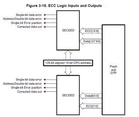
The TRM mention that only one of the SECDED modules (out of the two SECDED modules that work on lower 64 bits and upper 64 bits of a read 128-bit data) at a time can be tested.
Therefore, my understanding is that while testing the lower block a single bit error in the range 63:0 should trigger an error count but if a single bit error is injected in the upper block 127:64, while testing the lower block, it should not trigger an error count. However, it seems that it does.
I am trying to understand what is the purpose of having two blocks if the error is detected no matter where the error bit is located in the 128-bits data.
Does testing the Upper and Lower Block really matter or only one is enough to prove the functionality of the SECDED module?
Thank you
Laurent
