


Part Number: LAUNCHXL-F28379D
Hello, in previous forum here: LAUNCHXL-F28379D: Is there a way to synchronise the CMPSS, DC and TZ modules to the PWM frequency? - C2000 microcontrollers forum - C2000 ︎ microcontrollers - TI E2E support forums
I had been attempting to stop the PWM trips from clipping the signal mid-cycle, such that I always had 50% duty cycle.
Messing around with the rising and fall edge triggers of the GPIO enable signal, I have managed to get something working OK.
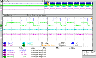
However, at what seems like random times, the PWM frequency of EPWM2B (yellow) and EPWM1B (green) will often seem to "latch" their duty cycle, or something similar, such that the frequency appears approximately twice that of the desired duty cycle. Here is a photo of the problem:

Complete code is below. This may help you to see the problem yourself and to help debug. I am using the Launchpad. I believe this is easier, rather select the code snippet, as I am unsure where this is coming from.
// Included Files.
#include "driverlib.h"
#include "device.h"

// Set PWM Frequency defines
#define EPWM_TIMER_TBPRD   600

// This sets the delay from receiving ENABLE to PWM switching start.
// This avoids very small duty cycle at charge start.
// Start with 10 microsecond delay.
#define ENABLE_DELAY_US 10

// Set maximum comparator trip value globally for now.
#define USER_DAC_REF 2000

// Sets number of charge cycles to be executed.
// This will be typically set to around 10, but for debug keep high.
#define NUM_OF_CHARGES 10

// Set PWM Function Prototypes.
void initEPWM1(void);
void initEPWM2(void);

// Comparator initialisation.
void initCMPSS(void);

// Set PWM Interrupt Functions.
__interrupt void epwm1ISR(void);
__interrupt void epwm2ISR(void);
__interrupt void risingEdgeTrigger(void);
__interrupt void fallingEdgeTrigger(void);

// Functions that set-up the GPIO signals.
void setupGPIO(void);

// Function that implements active-high complementary FED/RED.
void setupEPWMActiveHighComplementary(void);

// Setup Comparator Based Digital Compare Trips.
void setupCMPSSDigitalTrips(void);

// Define any and all ISR counters here.
uint16_t epwm1TZIntCount = 0;
uint16_t interruptCount1 = 0;
uint16_t chargeCount = 0;
uint16_t epwm1ISRCount = 0;
uint16_t epwm2ISRCount = 0;
uint16_t modifyCounterVal = 0;

uint16_t cpuTimer2IntCount =0;
uint16_t risingEdgeCount = 0;
uint16_t fallingEdgeCount = 0;

// Controlled phase variable for slave PWM module.
uint16_t PHASE_MODULATE_VAL = 0;

// Toggle reset occurs between rising and falling edges of GPIO to allow soft-start in CPU ISR.
uint16_t SS_RESET = 0;

// CPU timer interrupt
__interrupt void cpuTimer2ISR(void);

void initCPUTimers(void);
void configCPUTimer(uint32_t, float, float);

#define SS_INCREMENT 20
#define MAX_SS_VALUE 4095
uint16_t SOFT_START_VALUE = 0;
uint16_t LAST_SS_VALUE = 0;

void configureDAC(void);

int main(void)
{
    // As per usual, do all of these initialisation functions.
    // Initialise system, device clock, and peripherals
    Device_init();

    // Initialise PIE and clear PIE registers. Disables CPU interrupts.
    // and clear all CPU interrupt flags.
    Interrupt_initModule();

    // Disable pin locks and enable internal pull-ups.
    Device_initGPIO();

    // Initialise the PIE vector table with pointers to the shell interrupt
    // Service Routines (ISR).
    Interrupt_initVectorTable();

    // Specific GPIO Setup
    setupGPIO();

    GPIO_setInterruptType(GPIO_INT_XINT1, GPIO_INT_TYPE_RISING_EDGE);
    GPIO_setInterruptPin(5, GPIO_INT_XINT1);
    GPIO_enableInterrupt(GPIO_INT_XINT1);

    GPIO_setInterruptType(GPIO_INT_XINT2, GPIO_INT_TYPE_FALLING_EDGE);
    GPIO_setInterruptPin(5, GPIO_INT_XINT2);
    GPIO_enableInterrupt(GPIO_INT_XINT2);

    // Specify which function is called when an interrupt is triggered by assigning to register.
    Interrupt_register(INT_EPWM1, &epwm1ISR);
    Interrupt_register(INT_EPWM2, &epwm2ISR);

    // GPIO Timer Interrupts
    Interrupt_register(INT_XINT1, &risingEdgeTrigger);
    Interrupt_register(INT_XINT2, &fallingEdgeTrigger);

    // CPU Timer Interrupt for incrementing Soft-Start to max value at constant slope.
    Interrupt_register(INT_TIMER2, &cpuTimer2ISR);

    // Start EPWM Initialisation here, first disable peripheral.
    SysCtl_disablePeripheral(SYSCTL_PERIPH_CLK_TBCLKSYNC);

    // Initialise PWM1 with zero phase shift, set as master. See function.
    initEPWM1();

    // Initialise PWM2 with variable phase-shift, set as slave. See function.
    initEPWM2();

    // Set up digital compare trip-zones.
    setupCMPSSDigitalTrips();

    // Synchronised shadow load mode.
    EPWM_selectPeriodLoadEvent(EPWM2_BASE, EPWM_SHADOW_LOAD_MODE_SYNC);

    // Set initial phase-shift and time-base counter as zero for soft-start.
    EPWM_setPhaseShift(EPWM2_BASE, 0);
    EPWM_setTimeBaseCounter(EPWM2_BASE, 0);

    // Set EPWM1 SYNCO to be generated when counter is zero.
    EPWM_setSyncOutPulseMode(EPWM1_BASE, EPWM_SYNC_OUT_PULSE_ON_COUNTER_ZERO);

    // EPWM2 will use the EPWM1 SYNCO signal as SYNCIN value
    // Do not need to call setSyncInputConfig as EPWM2  uses this by default.
    EPWM_setSyncOutPulseMode(EPWM2_BASE, EPWM_SYNC_OUT_PULSE_ON_EPWMxSYNCIN);

    // Disable phase shift load for EPWM1, enable for PWM2.
    EPWM_disablePhaseShiftLoad(EPWM1_BASE);
    EPWM_enablePhaseShiftLoad(EPWM2_BASE);

    // Setup rising and falling edge delays for both modules.
    setupEPWMActiveHighComplementary();

    // Call comparator initialisation.
    initCMPSS();

    // Enable the synch register and lock to the PWM.
    SysCtl_enablePeripheral(SYSCTL_PERIPH_CLK_TBCLKSYNC);

    // Finally, enable the PWM interrupts.
    Interrupt_enable(INT_EPWM1);
    Interrupt_enable(INT_EPWM2);

    // Trip zone interrupts. Only use one and allow it to handle both PWM modules.
    //Interrupt_enable(INT_EPWM1_TZ);
    Interrupt_enable(INT_XINT1);
    Interrupt_enable(INT_XINT2);

    // Initialise device peripheral.
    initCPUTimers();

    // Configure CPU-Timer 2 to interrupt at X second intervals, ten microseconds.
    configCPUTimer(CPUTIMER2_BASE, DEVICE_SYSCLK_FREQ, 10);
    CPUTimer_enableInterrupt(CPUTIMER2_BASE);
    Interrupt_enable(INT_TIMER2);
    CPUTimer_startTimer(CPUTIMER2_BASE);

    // Configure DAC that measures analogue quantities for external view.
    configureDAC();

    // Enable Global Interrupt (INTM) and real time interrupt (DBGM)
    EINT;
    ERTM;

    // Loop forever to allow debug. 400Hz signal, 80% duty.
    for(;;)
    {
        while(chargeCount < NUM_OF_CHARGES) {
        // Charge enabled for maximum of 2 milliseconds.
        GPIO_writePin(67, 1);
        DEVICE_DELAY_US(2000);
        // Charging disabled for 500 microseconds.
        GPIO_writePin(67, 0);
        DEVICE_DELAY_US(500);
        chargeCount++;
        }

        // Simulate random delay between trigger pulse trains.
        DEVICE_DELAY_US(50000);
        chargeCount = 0;
    }
}

void setupCMPSSDigitalTrips(void) {

    // Disable all CBC trips for EPWMA/B of both modules.
    EPWM_disableTripZoneSignals(EPWM1_BASE, EPWM_TZ_SIGNAL_DCAEVT2);
    EPWM_disableTripZoneSignals(EPWM2_BASE, EPWM_TZ_SIGNAL_DCAEVT2);
    EPWM_disableTripZoneSignals(EPWM1_BASE, EPWM_TZ_SIGNAL_DCBEVT2);
    EPWM_disableTripZoneSignals(EPWM2_BASE, EPWM_TZ_SIGNAL_DCBEVT2);

    // Enable OST trips for EPWMA/B of both modules.
    EPWM_enableTripZoneSignals(EPWM1_BASE, EPWM_TZ_SIGNAL_DCAEVT1);
    EPWM_enableTripZoneSignals(EPWM2_BASE, EPWM_TZ_SIGNAL_DCAEVT1);
    EPWM_enableTripZoneSignals(EPWM1_BASE, EPWM_TZ_SIGNAL_DCBEVT1);
    EPWM_enableTripZoneSignals(EPWM2_BASE, EPWM_TZ_SIGNAL_DCBEVT1);

    // Trips 9 and 10 together cause DCAH.
    EPWM_selectDigitalCompareTripInput(EPWM1_BASE, EPWM_DC_TRIP_TRIPIN9, EPWM_DC_TYPE_DCAH);
    EPWM_selectDigitalCompareTripInput(EPWM1_BASE, EPWM_DC_TRIP_TRIPIN10, EPWM_DC_TYPE_DCBH);
    EPWM_selectDigitalCompareTripInput(EPWM2_BASE, EPWM_DC_TRIP_TRIPIN9, EPWM_DC_TYPE_DCAH);
    EPWM_selectDigitalCompareTripInput(EPWM2_BASE, EPWM_DC_TRIP_TRIPIN10, EPWM_DC_TYPE_DCBH);

    // Generate DCAEVT1 when DCAH high.
    EPWM_setTripZoneDigitalCompareEventCondition(EPWM1_BASE, EPWM_TZ_DC_OUTPUT_A1, EPWM_TZ_EVENT_DCXH_HIGH);
    EPWM_setTripZoneDigitalCompareEventCondition(EPWM2_BASE, EPWM_TZ_DC_OUTPUT_A1, EPWM_TZ_EVENT_DCXH_HIGH);
    EPWM_setTripZoneDigitalCompareEventCondition(EPWM1_BASE, EPWM_TZ_DC_OUTPUT_B1, EPWM_TZ_EVENT_DCXH_HIGH);
    EPWM_setTripZoneDigitalCompareEventCondition(EPWM2_BASE, EPWM_TZ_DC_OUTPUT_B1, EPWM_TZ_EVENT_DCXH_HIGH);

    // DCAEVT1 uses unfiltered version of DCAEVT1 for now.
    EPWM_setDigitalCompareEventSource(EPWM1_BASE, EPWM_DC_MODULE_A, EPWM_DC_EVENT_1, EPWM_DC_EVENT_SOURCE_ORIG_SIGNAL);
    EPWM_setDigitalCompareEventSource(EPWM2_BASE, EPWM_DC_MODULE_A, EPWM_DC_EVENT_1, EPWM_DC_EVENT_SOURCE_ORIG_SIGNAL);
    EPWM_setDigitalCompareEventSource(EPWM1_BASE, EPWM_DC_MODULE_B, EPWM_DC_EVENT_1, EPWM_DC_EVENT_SOURCE_ORIG_SIGNAL);
    EPWM_setDigitalCompareEventSource(EPWM2_BASE, EPWM_DC_MODULE_B, EPWM_DC_EVENT_1, EPWM_DC_EVENT_SOURCE_ORIG_SIGNAL);

    // DCAEVT1 is asynchronous
    EPWM_setDigitalCompareEventSyncMode(EPWM1_BASE, EPWM_DC_MODULE_A, EPWM_DC_EVENT_1, EPWM_DC_EVENT_INPUT_SYNCED);
    EPWM_setDigitalCompareEventSyncMode(EPWM2_BASE, EPWM_DC_MODULE_A, EPWM_DC_EVENT_1, EPWM_DC_EVENT_INPUT_SYNCED);
    EPWM_setDigitalCompareEventSyncMode(EPWM1_BASE, EPWM_DC_MODULE_B, EPWM_DC_EVENT_1, EPWM_DC_EVENT_INPUT_SYNCED);
    EPWM_setDigitalCompareEventSyncMode(EPWM2_BASE, EPWM_DC_MODULE_B, EPWM_DC_EVENT_1, EPWM_DC_EVENT_INPUT_SYNCED);

    // Force EPWM low action on DCAEVT1.
    EPWM_setTripZoneAction(EPWM1_BASE, EPWM_TZ_ACTION_EVENT_DCAEVT1, EPWM_TZ_ACTION_LOW);
    EPWM_setTripZoneAction(EPWM2_BASE, EPWM_TZ_ACTION_EVENT_DCAEVT1, EPWM_TZ_ACTION_LOW);
    EPWM_setTripZoneAction(EPWM1_BASE, EPWM_TZ_ACTION_EVENT_DCBEVT1, EPWM_TZ_ACTION_LOW);
    EPWM_setTripZoneAction(EPWM2_BASE, EPWM_TZ_ACTION_EVENT_DCBEVT1, EPWM_TZ_ACTION_LOW);

    // Enable Trip Zone Interrupt
    EPWM_enableTripZoneInterrupt(EPWM1_BASE, EPWM_TZ_INTERRUPT_DCAEVT1);
    EPWM_enableTripZoneInterrupt(EPWM1_BASE, EPWM_TZ_INTERRUPT_DCBEVT1);
}

void initEPWM1(void) {

    // Set up time-base clock.
    EPWM_setTimeBasePeriod(EPWM1_BASE, EPWM_TIMER_TBPRD);
    EPWM_setPhaseShift(EPWM1_BASE, 0);
    EPWM_setTimeBaseCounter(EPWM1_BASE, 0);

    // Counter compare config for EPWM1. May just need CMPA if use FED/RED.
    EPWM_setCounterCompareValue(EPWM1_BASE,
                                EPWM_COUNTER_COMPARE_A,
                                EPWM_TIMER_TBPRD/2);
    EPWM_setCounterCompareValue(EPWM1_BASE,
                                EPWM_COUNTER_COMPARE_B,
                                EPWM_TIMER_TBPRD/2);

    // Set up counter mode.
    EPWM_setTimeBaseCounterMode(EPWM1_BASE, EPWM_COUNTER_MODE_UP);
    EPWM_disablePhaseShiftLoad(EPWM1_BASE);
    EPWM_setClockPrescaler(EPWM1_BASE,
                           EPWM_CLOCK_DIVIDER_1,
                           EPWM_HSCLOCK_DIVIDER_1);

    // Set up PWM Shadowing. Load on CTR ZRO.
    EPWM_setCounterCompareShadowLoadMode(EPWM1_BASE,
                                         EPWM_COUNTER_COMPARE_A,
                                         EPWM_COMP_LOAD_ON_CNTR_ZERO);
    EPWM_setCounterCompareShadowLoadMode(EPWM1_BASE,
                                         EPWM_COUNTER_COMPARE_B,
                                         EPWM_COMP_LOAD_ON_CNTR_ZERO);

    // Set up the action qualifier.
    EPWM_setActionQualifierAction(EPWM1_BASE,
                                  EPWM_AQ_OUTPUT_A,
                                  EPWM_AQ_OUTPUT_HIGH,
                                  EPWM_AQ_OUTPUT_ON_TIMEBASE_ZERO);

    EPWM_setActionQualifierAction(EPWM1_BASE,
                                  EPWM_AQ_OUTPUT_B,
                                  EPWM_AQ_OUTPUT_LOW,
                                  EPWM_AQ_OUTPUT_ON_TIMEBASE_ZERO);

    EPWM_setActionQualifierAction(EPWM1_BASE,
                                  EPWM_AQ_OUTPUT_A,
                                  EPWM_AQ_OUTPUT_LOW,
                                  EPWM_AQ_OUTPUT_ON_TIMEBASE_UP_CMPA);

    EPWM_setActionQualifierAction(EPWM1_BASE,
                                  EPWM_AQ_OUTPUT_B,
                                  EPWM_AQ_OUTPUT_HIGH,
                                  EPWM_AQ_OUTPUT_ON_TIMEBASE_UP_CMPA);

    // // One-shot Active Low Trip ENABLE command - sets maximum charge time/minimum off time.
    EPWM_enableTripZoneSignals(EPWM1_BASE, EPWM_TZ_SIGNAL_OSHT1);
    EPWM_setTripZoneAction(EPWM1_BASE, EPWM_TZ_ACTION_EVENT_TZA, EPWM_TZ_ACTION_LOW);
    EPWM_setTripZoneAction(EPWM1_BASE, EPWM_TZ_ACTION_EVENT_TZB, EPWM_TZ_ACTION_LOW);
    EPWM_enableTripZoneInterrupt(EPWM1_BASE, EPWM_TZ_INTERRUPT_OST);

    // Clear latent trips.
    EPWM_clearTripZoneFlag(EPWM1_BASE, EPWM_TZ_INTERRUPT | EPWM_TZ_FLAG_OST);

    // Interrupt where we will change execute control code.
    // Select INT on time base counter zero event
    // Enable INT, but generate on the 15th event
    // Bandwidth is then FSW/15.
    EPWM_setInterruptSource(EPWM1_BASE, EPWM_INT_TBCTR_ZERO);
    EPWM_enableInterrupt(EPWM1_BASE);
    EPWM_setInterruptEventCount(EPWM1_BASE, 5);
}

void initEPWM2(void) {

    // Set up time-base clock.
    EPWM_setTimeBasePeriod(EPWM2_BASE, EPWM_TIMER_TBPRD);

    // Initially zero, but test with different TBPHS.
    // Ensure Time base is set to same value as phase shift.
    EPWM_setPhaseShift(EPWM2_BASE, 0);
    EPWM_setTimeBaseCounter(EPWM2_BASE, 0);

    // Counter compare configuration for EPWM2. May just need CMPA if use FED/RED.
    EPWM_setCounterCompareValue(EPWM2_BASE,
                                EPWM_COUNTER_COMPARE_A,
                                EPWM_TIMER_TBPRD/2);
    EPWM_setCounterCompareValue(EPWM2_BASE,
                                EPWM_COUNTER_COMPARE_B,
                                EPWM_TIMER_TBPRD/2);

    // Set up counter mode.
    EPWM_setTimeBaseCounterMode(EPWM2_BASE, EPWM_COUNTER_MODE_UP);
    EPWM_disablePhaseShiftLoad(EPWM2_BASE);
    EPWM_setClockPrescaler(EPWM2_BASE,
                           EPWM_CLOCK_DIVIDER_1,
                           EPWM_HSCLOCK_DIVIDER_1);

    // Set up PWM Shadowing. Load on CTR ZRO.
    EPWM_setCounterCompareShadowLoadMode(EPWM2_BASE,
                                         EPWM_COUNTER_COMPARE_A,
                                         EPWM_COMP_LOAD_ON_CNTR_ZERO);
    EPWM_setCounterCompareShadowLoadMode(EPWM2_BASE,
                                         EPWM_COUNTER_COMPARE_B,
                                         EPWM_COMP_LOAD_ON_CNTR_ZERO);

    // Set up the action qualifier.
    // Scope these and check if right, most likely need to be different to EPWM1.
    EPWM_setActionQualifierAction(EPWM2_BASE,
                                  EPWM_AQ_OUTPUT_A,
                                  EPWM_AQ_OUTPUT_HIGH,
                                  EPWM_AQ_OUTPUT_ON_TIMEBASE_ZERO);

    EPWM_setActionQualifierAction(EPWM2_BASE,
                                  EPWM_AQ_OUTPUT_B,
                                  EPWM_AQ_OUTPUT_LOW,
                                  EPWM_AQ_OUTPUT_ON_TIMEBASE_ZERO);

    EPWM_setActionQualifierAction(EPWM2_BASE,
                                  EPWM_AQ_OUTPUT_A,
                                  EPWM_AQ_OUTPUT_LOW,
                                  EPWM_AQ_OUTPUT_ON_TIMEBASE_UP_CMPA);

    EPWM_setActionQualifierAction(EPWM2_BASE,
                                  EPWM_AQ_OUTPUT_B,
                                  EPWM_AQ_OUTPUT_HIGH,
                                  EPWM_AQ_OUTPUT_ON_TIMEBASE_UP_CMPA);

    // One-shot Active Low Trip ENABLE command - sets maximum charge time/minimum off time.
    EPWM_enableTripZoneSignals(EPWM2_BASE, EPWM_TZ_SIGNAL_OSHT1);
    EPWM_setTripZoneAction(EPWM2_BASE, EPWM_TZ_ACTION_EVENT_TZA, EPWM_TZ_ACTION_LOW);
    EPWM_setTripZoneAction(EPWM2_BASE, EPWM_TZ_ACTION_EVENT_TZB, EPWM_TZ_ACTION_LOW);
    EPWM_disableTripZoneInterrupt(EPWM2_BASE, EPWM_TZ_INTERRUPT_OST);

    // Clear any latent trips.
    EPWM_clearTripZoneFlag(EPWM1_BASE, EPWM_TZ_INTERRUPT | EPWM_TZ_FLAG_OST);

    // Interrupt where we will change execute control code.
    // Select INT on time base counter zero event
    // Enable INT, but generate on the 15th event
    // Bandwidth is then FSW/15.
    EPWM_setInterruptSource(EPWM2_BASE, EPWM_INT_TBCTR_ZERO);
    EPWM_enableInterrupt(EPWM2_BASE);
    EPWM_setInterruptEventCount(EPWM2_BASE, 5);
}

void setupEPWMActiveHighComplementary() {

    // As always, use EPWMA as the input for both RED and FED.
    EPWM_setRisingEdgeDeadBandDelayInput(EPWM1_BASE, EPWM_DB_INPUT_EPWMA);
    EPWM_setRisingEdgeDeadBandDelayInput(EPWM2_BASE, EPWM_DB_INPUT_EPWMA);
    EPWM_setFallingEdgeDeadBandDelayInput(EPWM1_BASE, EPWM_DB_INPUT_EPWMA);
    EPWM_setFallingEdgeDeadBandDelayInput(EPWM2_BASE, EPWM_DB_INPUT_EPWMA);

    // Set the rising and falling edge delay values. One percent of switching period, for now.
    EPWM_setFallingEdgeDelayCount(EPWM1_BASE, EPWM_TIMER_TBPRD/100);
    EPWM_setFallingEdgeDelayCount(EPWM2_BASE, EPWM_TIMER_TBPRD/100);
    EPWM_setRisingEdgeDelayCount(EPWM1_BASE, EPWM_TIMER_TBPRD/100);
    EPWM_setRisingEdgeDelayCount(EPWM2_BASE, EPWM_TIMER_TBPRD/100);

    // Invert only the falling edge delayed output for active-high complementary mode.
    EPWM_setDeadBandDelayPolarity(EPWM1_BASE, EPWM_DB_RED, EPWM_DB_POLARITY_ACTIVE_HIGH);
    EPWM_setDeadBandDelayPolarity(EPWM1_BASE, EPWM_DB_FED, EPWM_DB_POLARITY_ACTIVE_LOW);
    EPWM_setDeadBandDelayPolarity(EPWM2_BASE, EPWM_DB_RED, EPWM_DB_POLARITY_ACTIVE_HIGH);
    EPWM_setDeadBandDelayPolarity(EPWM2_BASE, EPWM_DB_FED, EPWM_DB_POLARITY_ACTIVE_LOW);

    // Use the delayed signals instead of the original signals.
    EPWM_setDeadBandDelayMode(EPWM1_BASE, EPWM_DB_RED, true);
    EPWM_setDeadBandDelayMode(EPWM1_BASE, EPWM_DB_FED, true);
    EPWM_setDeadBandDelayMode(EPWM2_BASE, EPWM_DB_RED, true);
    EPWM_setDeadBandDelayMode(EPWM2_BASE, EPWM_DB_FED, true);

    // Importantly, do not switch output A with output B.
    EPWM_setDeadBandOutputSwapMode(EPWM1_BASE, EPWM_DB_OUTPUT_A, false);
    EPWM_setDeadBandOutputSwapMode(EPWM1_BASE, EPWM_DB_OUTPUT_B, false);
    EPWM_setDeadBandOutputSwapMode(EPWM2_BASE, EPWM_DB_OUTPUT_A, false);
    EPWM_setDeadBandOutputSwapMode(EPWM2_BASE, EPWM_DB_OUTPUT_B, false);
}

// Call this function to set-up the pin-out of the GPIOs.
void setupGPIO(void)
{
    // Enable PWM1A/B-2A/B on GPIO0-GPIO4
    GPIO_setPadConfig(0, GPIO_PIN_TYPE_STD);     // Standard push-pull output for PWM.
    GPIO_setPadConfig(1, GPIO_PIN_TYPE_STD);
    GPIO_setPadConfig(2, GPIO_PIN_TYPE_STD);
    GPIO_setPadConfig(3, GPIO_PIN_TYPE_STD);

    GPIO_setPinConfig(GPIO_0_EPWM1A);            // GPIO0 = PWM1A
    GPIO_setPinConfig(GPIO_1_EPWM1B);            // GPIO1 = PWM1B
    GPIO_setPinConfig(GPIO_2_EPWM2A);            // GPIO2 = PWM2A
    GPIO_setPinConfig(GPIO_3_EPWM2B);            // GPIO3 = PWM2B

    // Enable a GPIO67 output on GPIO67, set it high
    GPIO_setPadConfig(67, GPIO_PIN_TYPE_PULLUP); // Enable pullup on GPIO67
    GPIO_writePin(67, 1);                            // Load output latch
    GPIO_setPinConfig(GPIO_67_GPIO67);                // GPIO67 = GPIO67
    GPIO_setDirectionMode(67, GPIO_DIR_MODE_OUT);    // GPIO67 = output

    // Enable a GPIO output on GPIO8, set it high
    GPIO_setPadConfig(5, GPIO_PIN_TYPE_PULLUP);     // Enable pullup on GPIO5
    GPIO_setPinConfig(GPIO_5_GPIO5);                // GPIO5 = GPIO5 MUX SELECT
    GPIO_setDirectionMode(5, GPIO_DIR_MODE_IN);     // GPIO5 = input (output overvolts latch)

    // Enable Trip Zone input on GPIO5
    GPIO_setQualificationMode(5, GPIO_QUAL_SYNC); // sync input

    // Input pins trigger XBAR TZs
    XBAR_setInputPin(XBAR_INPUT1, 5);              // GPIO5 = TZ1

}

void initCMPSS(void) {

    // Enable the CMPSS and configure the negative reference to be fed from the DAC.
    // CMPSS1 is not used as it's CMPIN is shorted to the DACREF.
    // Input/Output Over-voltage
    CMPSS_enableModule(CMPSS2_BASE);
    CMPSS_configHighComparator(CMPSS2_BASE, CMPSS_INSRC_DAC);
    CMPSS_enableModule(CMPSS3_BASE);
    CMPSS_configHighComparator(CMPSS3_BASE, CMPSS_INSRC_DAC);

    // Input/Output Over-current.
    CMPSS_enableModule(CMPSS5_BASE);
    CMPSS_configHighComparator(CMPSS5_BASE, CMPSS_INSRC_DAC);
    CMPSS_enableModule(CMPSS6_BASE);
    CMPSS_configHighComparator(CMPSS6_BASE, CMPSS_INSRC_DAC);

    // Set DAC reference as VDDA, and set the required trip value.
    CMPSS_configDAC(CMPSS2_BASE, CMPSS_DACREF_VDDA
                    | CMPSS_DACVAL_SYSCLK | CMPSS_DACSRC_SHDW);
    CMPSS_setDACValueHigh(CMPSS2_BASE, USER_DAC_REF);
    CMPSS_configDAC(CMPSS3_BASE, CMPSS_DACREF_VDDA
                    | CMPSS_DACVAL_SYSCLK | CMPSS_DACSRC_SHDW);
    CMPSS_setDACValueHigh(CMPSS3_BASE, USER_DAC_REF);
    CMPSS_configDAC(CMPSS5_BASE, CMPSS_DACREF_VDDA
                    | CMPSS_DACVAL_SYSCLK | CMPSS_DACSRC_SHDW);
    CMPSS_setDACValueHigh(CMPSS5_BASE, USER_DAC_REF);
    CMPSS_configDAC(CMPSS6_BASE, CMPSS_DACREF_VDDA
                    | CMPSS_DACVAL_SYSCLK | CMPSS_DACSRC_SHDW);
    CMPSS_setDACValueHigh(CMPSS6_BASE, USER_DAC_REF);

    // Configure now the digital filter. Use max clock pre-scale, sample window size, and threshold.
    CMPSS_configFilterHigh(CMPSS2_BASE, 0x3FF, 32, 31);
    CMPSS_configFilterHigh(CMPSS3_BASE, 0x3FF, 32, 31);
    CMPSS_configFilterHigh(CMPSS5_BASE, 0x3FF, 32, 31);
    CMPSS_configFilterHigh(CMPSS6_BASE, 0x3FF, 32, 31);

    // Initialise filter logic and begin filtering
    CMPSS_initFilterHigh(CMPSS2_BASE);
    CMPSS_initFilterHigh(CMPSS3_BASE);
    CMPSS_initFilterHigh(CMPSS5_BASE);
    CMPSS_initFilterHigh(CMPSS6_BASE);

    // Configure the output signals. CTRIPH, which feeds into the PWM X-BAR, need only be generated.
    // CTRIPH will be fed with the asynchronous comparator output.
    CMPSS_configOutputsHigh(CMPSS2_BASE, CMPSS_TRIP_FILTER);
    CMPSS_configOutputsHigh(CMPSS3_BASE, CMPSS_TRIP_FILTER);
    CMPSS_configOutputsHigh(CMPSS5_BASE, CMPSS_TRIP_FILTER);
    CMPSS_configOutputsHigh(CMPSS6_BASE, CMPSS_TRIP_FILTER);

    // Here is the important part, set the output mux configs.
    XBAR_setEPWMMuxConfig(XBAR_TRIP9, XBAR_EPWM_MUX02_CMPSS2_CTRIPH);
    XBAR_setEPWMMuxConfig(XBAR_TRIP10, XBAR_EPWM_MUX04_CMPSS3_CTRIPH);
    XBAR_setEPWMMuxConfig(XBAR_TRIP11, XBAR_EPWM_MUX08_CMPSS5_CTRIPH);
    XBAR_setEPWMMuxConfig(XBAR_TRIP12, XBAR_EPWM_MUX10_CMPSS6_CTRIPH);

    XBAR_enableEPWMMux(XBAR_TRIP9, XBAR_MUX02);
    XBAR_enableEPWMMux(XBAR_TRIP10, XBAR_MUX04);
    XBAR_enableEPWMMux(XBAR_TRIP11, XBAR_MUX08);
    XBAR_enableEPWMMux(XBAR_TRIP12, XBAR_MUX10);

    // Set typical hysteresis on comparator inputs.
    CMPSS_setHysteresis(CMPSS2_BASE, 4);
    CMPSS_setHysteresis(CMPSS3_BASE, 4);
    CMPSS_setHysteresis(CMPSS5_BASE, 4);
    CMPSS_setHysteresis(CMPSS6_BASE, 4);

}

// Configure DAC - Setup the reference voltage and output value for the DAC
void configureDAC(void)
{
    // Use ADC reference voltage.
    DAC_setReferenceVoltage(DACA_BASE, DAC_REF_ADC_VREFHI);

    // Enable the DAC output
    DAC_enableOutput(DACA_BASE);

    // Set the DAC shadow output to 0
    DAC_setShadowValue(DACA_BASE, 0);

    // Load on next SYSCLOCK
    DAC_setLoadMode(DACA_BASE, DAC_LOAD_SYSCLK);

    // Delay for buffered DAC to power up
    DEVICE_DELAY_US(10);
}

void initCPUTimers(void) {
    // Initialise timer period to max
    CPUTimer_setPeriod(CPUTIMER2_BASE, 0xFFFFFFFF);

    // Initialise pre-scale counter to divide by 1 SYSCLKOUT
    CPUTimer_setPreScaler(CPUTIMER2_BASE, 0);

    // Stop timer
    CPUTimer_stopTimer(CPUTIMER2_BASE);

    // Reload counter register with period value
    CPUTimer_reloadTimerCounter(CPUTIMER2_BASE);

    // Reset any latent interrupt counts
    cpuTimer2IntCount = 0;
}

void configCPUTimer(uint32_t cpuTimer, float freq, float period)
{
    uint32_t temp;

    // Initialise timer period:
    temp = (uint32_t)(freq / 1000000 * period);
    CPUTimer_setPeriod(cpuTimer, temp);

    // Set pre-scale counter to divide by 1 (SYSCLKOUT):
    CPUTimer_setPreScaler(cpuTimer, 0);

    // Initialises timer control register. The timer is stopped, reloaded,
    // free run disabled, and interrupt enabled.
    // Additionally, the free and soft bits are set
    CPUTimer_stopTimer(cpuTimer);
    CPUTimer_reloadTimerCounter(cpuTimer);
    CPUTimer_setEmulationMode(cpuTimer,
                              CPUTIMER_EMULATIONMODE_RUNFREE);
    CPUTimer_enableInterrupt(cpuTimer);
}


__interrupt void epwm1ISR() {
epwm1ISRCount++;

// Modulate phase-shift register and time-base shift too.
PHASE_MODULATE_VAL = PHASE_MODULATE_VAL + 5;
if(PHASE_MODULATE_VAL > EPWM_TIMER_TBPRD/2) {
    PHASE_MODULATE_VAL = EPWM_TIMER_TBPRD/2;
}

EPWM_setPhaseShift(EPWM2_BASE, PHASE_MODULATE_VAL);

// Clear INT flag for this timer
EPWM_clearEventTriggerInterruptFlag(EPWM1_BASE);

// Acknowledge interrupt group
Interrupt_clearACKGroup(INTERRUPT_ACK_GROUP3);
}

__interrupt void epwm2ISR() {
epwm2ISRCount++;

// Clear INT flag for this timer
EPWM_clearEventTriggerInterruptFlag(EPWM2_BASE);

// Acknowledge interrupt group
Interrupt_clearACKGroup(INTERRUPT_ACK_GROUP3);
}

__interrupt void risingEdgeTrigger(void)
{
    risingEdgeCount++;

    // Blank a switching period after trip
    DEVICE_DELAY_US(10);

    PHASE_MODULATE_VAL = 0;

    // Before initiation of new soft-start cycle, reset to zero phase-shift and zero counter.
    // Reset counters for both EPWM1 and EPWM2.
    EPWM_setTimeBasePeriod(EPWM1_BASE, EPWM_TIMER_TBPRD);
    EPWM_setTimeBasePeriod(EPWM2_BASE, EPWM_TIMER_TBPRD);
    EPWM_setTimeBaseCounter(EPWM1_BASE, 0);
    EPWM_setTimeBaseCounter(EPWM2_BASE, 0);
    EPWM_setPhaseShift(EPWM2_BASE, 0);

    // For one-shot trips, we must re-enable all of the trip-zone flags within both PWM modules.
    EPWM_clearTripZoneFlag(EPWM1_BASE, (EPWM_TZ_INTERRUPT | EPWM_TZ_FLAG_OST | EPWM_TZ_FLAG_DCAEVT1 | EPWM_TZ_FLAG_DCBEVT1));
    EPWM_clearTripZoneFlag(EPWM2_BASE, (EPWM_TZ_INTERRUPT | EPWM_TZ_FLAG_OST | EPWM_TZ_FLAG_DCAEVT1 | EPWM_TZ_FLAG_DCBEVT1));

    // Re-enable CPU timer at rising edge to allow soft-start
    CPUTimer_startTimer(CPUTIMER2_BASE);

    // Acknowledge this interrupt to receive more interrupts from group 2
    Interrupt_clearACKGroup(INTERRUPT_ACK_GROUP2);
    Interrupt_clearACKGroup(INTERRUPT_ACK_GROUP1);
}

__interrupt void fallingEdgeTrigger(void) {

    // Small delay...
    DEVICE_DELAY_US(10);

    fallingEdgeCount++;
    SS_RESET = 1;

    PHASE_MODULATE_VAL = 0;

    // Set soft-start DAC value to zero
    DAC_setShadowValue(DACA_BASE, 0);

    // Disable CPU timer 2 which so it doesn't increment during pulse disable
    CPUTimer_stopTimer(CPUTIMER2_BASE);

    // Clear GPIO falling edge interrupt.
    Interrupt_clearACKGroup(INTERRUPT_ACK_GROUP1);
}

__interrupt void cpuTimer2ISR(void) {
    cpuTimer2IntCount++;

    // Reset the soft-start to zero, reset controller phase-shift to zero.
    if(SS_RESET == 1) {
        SOFT_START_VALUE = 0;
    }

    SS_RESET = 0;

    // At every counter event, increment soft-start value.
    SOFT_START_VALUE = SOFT_START_VALUE + SS_INCREMENT;

    // Keep at maximum in CPU interrupt until external trigger reset.
    if(SOFT_START_VALUE  > MAX_SS_VALUE) {
        SOFT_START_VALUE = 4095;
    }

    // Pass value to DAC-A here, soft-start on rising-edge enable.
    DAC_setShadowValue(DACA_BASE, SOFT_START_VALUE);
}
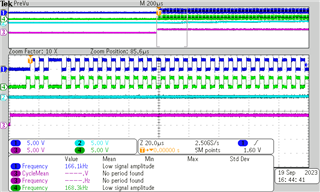
Since I use active-high complementary PWM dead-band, this unfortunately also messes up my EPWMxA/xB relations as shown below:
Best regards,
JMH.


