This thread has been locked.

If you have a related question, please click the "Ask a related question" button in the top right corner. The newly created question will be automatically linked to this question.

TMDSCNCD28P65X: EPWM synchronisation

Part Number: TMDSCNCD28P65X


Hello Everyone,

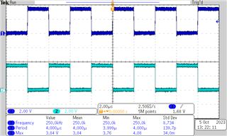
I am trying to configure EPWM module for TMDSCNCD28P65X control card, but having some issue in EPWM synchronisation. I have called configured EPWM 1 and EPWM 2 as follows for

EALLOW;
CpuSysRegs.PCLKCR0.bit.TBCLKSYNC = 0;
EDIS;

EPwm1_Init();
EPwm2_Init();
EPwm3_Init();
EPwm5_Init();
EPwm18_Init();

EALLOW;
CpuSysRegs.PCLKCR0.bit.TBCLKSYNC = 1;
EDIS;

However, there is some phase delay of approximately 20n sec between the two module. Please note I have enable phase register for both EPWM 1 and EMPW 2 and set it to zero. In order to circumvent this problem I have configured EMPW 18 to act as a clk source for EPWM 1 and EMPM 2, in this case both the 1&2 are synced. I want to understand why TBCLKSYNC is not synchronizing the EPWM module. 

  • Hi Manish,

    Could you disable phase register for ePWM1? If ePWM1 is your primary module that is syncing the other PWM modules. Also before you call CpuSysRegs.PCLKCR0.bit.TBCLKSYNC could you call, GTBCLKSYNC and set that to 1? This should help synchronize the modules.

    Best,

    Ryan Ma

  • Hi Ryan, 

    Thank you for the quick response. I have already tried setting GTBCLKSYNC to 1. This indeed sync all the PWM module. However, in this case the phase register values seems to have no effect i.e. if I enable phase loading for PWM2 and assign some value in the phase register, still there is no phase shift when GTBCLKSYNC is set to 1

    Regards,

    Manish Kumar

  • Hi Manish,

    Are you enabling shadow load mode for PWM2? If so, can you verify when writing to the TBPHS register that it gets updated in the CCS register window. When are you syncing PWM modules on TBCTR = ZRO ... etc? You need to generate some kind of software sync from ePWM1 to ePWM2 in order to load TBPHS to the TBCTR value. Also make sure that ePWM2 syncin is ePWM1's syncout. 

    Best,

    Ryan Ma

  • Hi Ryan

    This is the code that I am trying to implement

    void main(void)

    {
    //
    // Initialisation of System Control:

    InitSysCtrl();

    //
    // Enable PWM1, PWM2 and PWM3
    //
    CpuSysRegs.PCLKCR2.bit.EPWM1=1;
    CpuSysRegs.PCLKCR2.bit.EPWM2=1;
    //
    // Initialisation of GPIO pins for ePWM1, ePWM2, ePWM4, ePWM5

    EPwm1_Gpio_Config();
    EPwm2_Gpio_Config();

    //
    // Disable CPU interrupts and clear all CPU interrupt flags:
    //
    IER = 0;
    IFR = 0;

    //
    // Initialisation of ePWM Module
    //
    EALLOW;
    CpuSysRegs.PCLKCR0.bit.TBCLKSYNC = 0;
    CpuSysRegs.PCLKCR0.bit.GTBCLKSYNC = 0;
    EDIS;

    EPwm1_Init();
    EPwm2_Init();

    EALLOW;
    CpuSysRegs.PCLKCR0.bit.GTBCLKSYNC = 1;
    CpuSysRegs.PCLKCR0.bit.TBCLKSYNC = 1;
    EDIS;

    //
    // Enable global Interrupts and higher priority real-time debug events:
    //
    EINT; // Enable Global interrupt INTM
    ERTM; // Enable Global realtime interrupt DBGM

    //
    // Loop forever:
    //
    for(;;)
    {
    asm (" NOP");
    EPwm2Regs.TBPHS.bit.TBPHS = val;
    }
    }


    void EPwm1_Init()
    {
    //
    // Setup TBCLK
    //
    EPwm1Regs.EPWMSYNCOUTEN.bit.ZEROEN=1;
    EPwm1Regs.TBCTR = 0; // Clear counter
    EPwm1Regs.TBCTL.bit.CTRMODE = 2; // Count up-down
    EPwm1Regs.TBPRD = 250; // Timer period for 200 kHz
    EPwm1Regs.TBCTL.bit.PHSEN = 0; // Disable phase loading
    EPwm1Regs.TBPHS.bit.TBPHS = 0; // Phase is 0

    EPwm1Regs.TBCTL.bit.HSPCLKDIV = 0; // Clock ratio
    EPwm1Regs.TBCTL.bit.CLKDIV = 0;
    //
    //Shadow register is set to load on CTR=ZERO
    //
    EPwm1Regs.CMPCTL.bit.SHDWAMODE = 0; // EPWM1A_SHADOW_MODE
    EPwm1Regs.CMPCTL.bit.SHDWBMODE = 0; // EPWM1B_SHADOW_MODE
    EPwm1Regs.CMPCTL.bit.LOADAMODE = 2; // EPWM1A_Load_CTR_ZERO
    EPwm1Regs.CMPCTL.bit.LOADBMODE = 2; // EPWM1B_Load_CTR_ZERO
    //
    // Set Compare values
    //
    EPwm1Regs.CMPA.bit.CMPA = 125; // Set compare A value
    //
    // Set actions
    //
    EPwm1Regs.AQCTLA.bit.CAU = AQ_SET; // Set PWM1A on Zero
    EPwm1Regs.AQCTLA.bit.CAD = AQ_CLEAR; // Clear PWM1A on event A,
    // up count

    }


    void EPwm2_Init()
    {
    //
    // Setup TBCLK
    //
    EPwm2Regs.TBCTR = 0; // Clear counter
    EPwm2Regs.EPWMSYNCINSEL.bit.SEL = 1;
    EPwm2Regs.TBCTL.bit.CTRMODE = 2; // Count up-down
    EPwm2Regs.TBPRD = 250; // Timer period for 200 kHz
    EPwm2Regs.TBCTL.bit.PHSEN = 1; // Disable phase loading
    EPwm2Regs.TBPHS.bit.TBPHS = 0; // Phase is 0
    EPwm2Regs.TBCTL.bit.HSPCLKDIV = 0; // Clock ratio
    EPwm2Regs.TBCTL.bit.CLKDIV = 0;
    //
    //Shadow register is set to load on CTR=ZERO
    //
    EPwm2Regs.CMPCTL.bit.SHDWAMODE = 0; // EPWM1A_SHADOW_MODE
    EPwm2Regs.CMPCTL.bit.SHDWBMODE = 0; // EPWM1B_SHADOW_MODE
    EPwm2Regs.CMPCTL.bit.LOADAMODE = 2; // EPWM1A_Load_CTR_ZERO
    EPwm2Regs.CMPCTL.bit.LOADBMODE = 2; // EPWM1B_Load_CTR_ZERO
    //
    // Set Compare values
    //
    EPwm2Regs.CMPA.bit.CMPA = 125; // Set compare A value
    //
    // Set actions
    //
    EPwm2Regs.AQCTLA.bit.CAU = AQ_SET; // Set PWM1A on Zero
    EPwm2Regs.AQCTLA.bit.CAD = AQ_CLEAR; // Clear PWM1A on event A,
    // up count

    }

    So the EPWM1 sync out is sync in for EPWM2 yet there is inherent delay in the PWM module. Yellow one is EPWM1A and Magenta is EPWM2A.

  • Hi Manish,

    Here is my code snippet, the only thing I changed was the TBPHS value to be 250, so it produced a 180 degree phase shift.

    //
    // Included Files
    //
    #include "f28x_project.h"
    
    //
    // Globals
    //
    typedef struct
    {
        volatile struct EPWM_REGS *EPwmRegHandle;
        Uint16 EPwm_CMPA_Direction;
        Uint16 EPwm_CMPB_Direction;
        Uint16 EPwmTimerIntCount;
        Uint16 EPwmMaxCMPA;
        Uint16 EPwmMinCMPA;
        Uint16 EPwmMaxCMPB;
        Uint16 EPwmMinCMPB;
    }EPWM_INFO;
    
    EPWM_INFO epwm1_info;
    EPWM_INFO epwm2_info;
    EPWM_INFO epwm3_info;


    //
    // Main
    //
    void main(void)
    {
    //
    // Step 1. Initialize System Control:
    // PLL, WatchDog, enable Peripheral Clocks
    // This example function is found in the f2838x_sysctrl.c file.
    //
        InitSysCtrl();
    
    //
    // Step 2. Initialize GPIO:
    // This example function is found in the f2838x_gpio.c file and
    // illustrates how to set the GPIO to it's default state.
    //
    //    InitGpio();
    
    //
    // enable PWM1, PWM2 and PWM3
    //
        CpuSysRegs.PCLKCR2.bit.EPWM1=1;
        CpuSysRegs.PCLKCR2.bit.EPWM2=1;
        CpuSysRegs.PCLKCR2.bit.EPWM3=1;
    
    //
    // For this case just init GPIO pins for ePWM1, ePWM2, ePWM3
    // These functions are in the f2838x_epwm.c file
    //
        InitEPwm1Gpio();
        InitEPwm2Gpio();
        InitEPwm3Gpio();
    
    //
    // Step 3. Clear all interrupts and initialize PIE vector table:
    // Disable CPU interrupts
    //
        DINT;
    
    //
    // Initialize the PIE control registers to their default state.
    // The default state is all PIE interrupts disabled and flags
    // are cleared.
    // This function is found in the f2838x_piectrl.c file.
    //
        InitPieCtrl();
    
    //
    // Disable CPU interrupts and clear all CPU interrupt flags:
    //
        IER = 0x0000;
        IFR = 0x0000;
    
    //
    // Initialize the PIE vector table with pointers to the shell Interrupt
    // Service Routines (ISR).
    // This will populate the entire table, even if the interrupt
    // is not used in this example.  This is useful for debug purposes.
    // The shell ISR routines are found in f2838x_defaultisr.c.
    // This function is found in f2838x_pievect.c.
    //
        InitPieVectTable();
    
    //
    // Interrupts that are used in this example are re-mapped to
    // ISR functions found within this file.
    //
        EALLOW; // This is needed to write to EALLOW protected registers
    
        EDIS;   // This is needed to disable write to EALLOW protected registers
    
    //
    // For this example, only initialize the ePWM
    //
        EALLOW;
        CpuSysRegs.PCLKCR0.bit.TBCLKSYNC = 0;
        CpuSysRegs.PCLKCR0.bit.GTBCLKSYNC = 0;
        EDIS;
    
        EPwm1_Init();
        EPwm2_Init();
    
        EALLOW;
        CpuSysRegs.PCLKCR0.bit.GTBCLKSYNC = 1;
        CpuSysRegs.PCLKCR0.bit.TBCLKSYNC = 1;
        EDIS;
    //
    // Step 4. User specific code, enable interrupts:
    //
    
    //
    // Enable CPU INT3 which is connected to EPWM1-3 INT:
    //
        IER |= M_INT3;
    
    //
    // Enable EPWM INTn in the PIE: Group 3 interrupt 1-3
    //
        PieCtrlRegs.PIEIER3.bit.INTx1 = 1;
        PieCtrlRegs.PIEIER3.bit.INTx2 = 1;
        PieCtrlRegs.PIEIER3.bit.INTx3 = 1;
    
    //
    // Enable global Interrupts and higher priority real-time debug events:
    //
        EINT;  // Enable Global interrupt INTM
        ERTM;  // Enable Global realtime interrupt DBGM
    
    //
    // Step 5. IDLE loop. Just sit and loop forever (optional):
    //
        //
        // Loop forever:
        //
        for(;;)
        {
            asm (" NOP");
            EPwm2Regs.TBPHS.bit.TBPHS = 250;
        }
    }
    void EPwm1_Init()
    {
    //
    // Setup TBCLK
    //
    EPwm1Regs.EPWMSYNCOUTEN.bit.ZEROEN=1;
    EPwm1Regs.TBCTR = 0; // Clear counter
    EPwm1Regs.TBCTL.bit.CTRMODE = 2; // Count up-down
    EPwm1Regs.TBPRD = 250; // Timer period for 200 kHz
    EPwm1Regs.TBCTL.bit.PHSEN = 0; // Disable phase loading
    EPwm1Regs.TBPHS.bit.TBPHS = 0; // Phase is 0
    
    EPwm1Regs.TBCTL.bit.HSPCLKDIV = 0; // Clock ratio
    EPwm1Regs.TBCTL.bit.CLKDIV = 0;
    //
    //Shadow register is set to load on CTR=ZERO
    //
    EPwm1Regs.CMPCTL.bit.SHDWAMODE = 0; // EPWM1A_SHADOW_MODE
    EPwm1Regs.CMPCTL.bit.SHDWBMODE = 0; // EPWM1B_SHADOW_MODE
    EPwm1Regs.CMPCTL.bit.LOADAMODE = 2; // EPWM1A_Load_CTR_ZERO
    EPwm1Regs.CMPCTL.bit.LOADBMODE = 2; // EPWM1B_Load_CTR_ZERO
    //
    // Set Compare values
    //
    EPwm1Regs.CMPA.bit.CMPA = 125; // Set compare A value
    //
    // Set actions
    //
    EPwm1Regs.AQCTLA.bit.CAU = AQ_SET; // Set PWM1A on Zero
    EPwm1Regs.AQCTLA.bit.CAD = AQ_CLEAR; // Clear PWM1A on event A,
    // up count
    
    }
    
    
    void EPwm2_Init()
    {
    //
    // Setup TBCLK
    //
    EPwm2Regs.TBCTR = 0; // Clear counter
    EPwm2Regs.EPWMSYNCINSEL.bit.SEL = 1;
    EPwm2Regs.TBCTL.bit.CTRMODE = 2; // Count up-down
    EPwm2Regs.TBPRD = 250; // Timer period for 200 kHz
    EPwm2Regs.TBCTL.bit.PHSEN = 1; // Disable phase loading
    EPwm2Regs.TBPHS.bit.TBPHS = 0; // Phase is 0
    EPwm2Regs.TBCTL.bit.HSPCLKDIV = 0; // Clock ratio
    EPwm2Regs.TBCTL.bit.CLKDIV = 0;
    //
    //Shadow register is set to load on CTR=ZERO
    //
    EPwm2Regs.CMPCTL.bit.SHDWAMODE = 0; // EPWM1A_SHADOW_MODE
    EPwm2Regs.CMPCTL.bit.SHDWBMODE = 0; // EPWM1B_SHADOW_MODE
    EPwm2Regs.CMPCTL.bit.LOADAMODE = 2; // EPWM1A_Load_CTR_ZERO
    EPwm2Regs.CMPCTL.bit.LOADBMODE = 2; // EPWM1B_Load_CTR_ZERO
    //
    // Set Compare values
    //
    EPwm2Regs.CMPA.bit.CMPA = 125; // Set compare A value
    //
    // Set actions
    //
    EPwm2Regs.AQCTLA.bit.CAU = AQ_SET; // Set PWM1A on Zero
    EPwm2Regs.AQCTLA.bit.CAD = AQ_CLEAR; // Clear PWM1A on event A,
    // up count
    
    }
    //
    // End of file
    //
    

    This is the results I am seeing on the scope: Can you confirm?

    Here is also a register export of ePWM1 and 2 configurations. Please compare with your registers to see if there is anything different.

    521177 40
    R EPwm1Regs_TBCTL 0x0000000F 0x0002
    R EPwm1Regs_TBCTL2 0x0000000F 0x0000
    R EPwm1Regs_EPWMSYNCINSEL 0x0000000F 0x0001
    R EPwm1Regs_TBCTR 0x0000000F 0x0005
    R EPwm1Regs_TBSTS 0x0000000F 0x0000
    R EPwm1Regs_EPWMSYNCOUTEN 0x0000000F 0x0003
    R EPwm1Regs_TBCTL3 0x0000000F 0x0000
    R EPwm1Regs_CMPCTL 0x0000000F 0x000A
    R EPwm1Regs_CMPCTL2 0x0000000F 0x0000
    R EPwm1Regs_DBCTL 0x0000000F 0x0000
    R EPwm1Regs_DBCTL2 0x0000000F 0x0000
    R EPwm1Regs_AQCTL 0x0000000F 0x0000
    R EPwm1Regs_AQTSRCSEL 0x0000000F 0x0000
    R EPwm1Regs_PCCTL 0x0000000F 0x0000
    R EPwm1Regs_VCAPCTL 0x0000000F 0x0000
    R EPwm1Regs_VCNTCFG 0x0000000F 0x0000
    R EPwm1Regs_HRCNFG 0x0000000F 0x0000
    R EPwm1Regs_HRCNFG2 0x0000000F 0x0000
    R EPwm1Regs_HRPCTL 0x0000000F 0x0000
    R EPwm1Regs_TRREM 0x0000000F 0x0000
    R EPwm1Regs_GLDCTL 0x0000000F 0x0000
    R EPwm1Regs_GLDCFG 0x0000000F 0x0000
    R EPwm1Regs_EPWMXLINK 0x0000000B 0x00000000
    R EPwm1Regs_EPWMXLINK2 0x0000000B 0x00000000
    R EPwm1Regs_AQCTLA 0x0000000F 0x0060
    R EPwm1Regs_AQCTLA2 0x0000000F 0x0000
    R EPwm1Regs_AQCTLB 0x0000000F 0x0000
    R EPwm1Regs_AQCTLB2 0x0000000F 0x0000
    R EPwm1Regs_AQSFRC 0x0000000F 0x0000
    R EPwm1Regs_AQCSFRC 0x0000000F 0x0000
    R EPwm1Regs_DBREDHR 0x0000000F 0x0000
    R EPwm1Regs_DBRED 0x0000000F 0x0000
    R EPwm1Regs_DBFEDHR 0x0000000F 0x0000
    R EPwm1Regs_DBFED 0x0000000F 0x0000
    R EPwm1Regs_TBPHS 0x0000000B 0x00000000
    R EPwm1Regs_TBPRDHR 0x0000000F 0x0000
    R EPwm1Regs_TBPRD 0x0000000F 0x00FA
    R EPwm1Regs_CMPA 0x0000000B 0x007D0000
    R EPwm1Regs_CMPB 0x0000000B 0x00000000
    R EPwm1Regs_CMPC 0x0000000F 0x0000
    R EPwm1Regs_CMPD 0x0000000F 0x0000
    R EPwm1Regs_GLDCTL2 0x0000000F 0x0000
    R EPwm1Regs_SWVDELVAL 0x0000000F 0x0000
    R EPwm1Regs_TZSEL 0x0000000F 0x0000
    R EPwm1Regs_TZSEL2 0x0000000F 0x0000
    R EPwm1Regs_TZDCSEL 0x0000000F 0x0000
    R EPwm1Regs_TZCTL 0x0000000F 0x0000
    R EPwm1Regs_TZCTL2 0x0000000F 0x0000
    R EPwm1Regs_TZCTLDCA 0x0000000F 0x0000
    R EPwm1Regs_TZCTLDCB 0x0000000F 0x0000
    R EPwm1Regs_TZEINT 0x0000000F 0x0000
    R EPwm1Regs_TZFLG 0x0000000F 0x0000
    R EPwm1Regs_TZCBCFLG 0x0000000F 0x0000
    R EPwm1Regs_TZOSTFLG 0x0000000F 0x0000
    R EPwm1Regs_TZCLR 0x0000000F 0x0000
    R EPwm1Regs_TZCBCCLR 0x0000000F 0x0000
    R EPwm1Regs_TZOSTCLR 0x0000000F 0x0000
    R EPwm1Regs_TZFRC 0x0000000F 0x0000
    R EPwm1Regs_TZTRIPOUTSEL 0x0000000F 0x0000
    R EPwm1Regs_ETSEL 0x0000000F 0x0000
    R EPwm1Regs_ETPS 0x0000000F 0x0000
    R EPwm1Regs_ETFLG 0x0000000F 0x0000
    R EPwm1Regs_ETCLR 0x0000000F 0x0000
    R EPwm1Regs_ETFRC 0x0000000F 0x0000
    R EPwm1Regs_ETINTPS 0x0000000F 0x0000
    R EPwm1Regs_ETSOCPS 0x0000000F 0x0000
    R EPwm1Regs_ETCNTINITCTL 0x0000000F 0x0000
    R EPwm1Regs_ETCNTINIT 0x0000000F 0x0000
    R EPwm1Regs_ETINTMIXEN 0x0000000F 0x0003
    R EPwm1Regs_ETSOCAMIXEN 0x0000000F 0x0003
    R EPwm1Regs_ETSOCBMIXEN 0x0000000F 0x0003
    R EPwm1Regs_DCTRIPSEL 0x0000000F 0x0000
    R EPwm1Regs_DCACTL 0x0000000F 0x0000
    R EPwm1Regs_DCBCTL 0x0000000F 0x0000
    R EPwm1Regs_DCFCTL 0x0000000F 0x0000
    R EPwm1Regs_DCCAPCTL 0x0000000F 0x0000
    R EPwm1Regs_DCFOFFSET 0x0000000F 0x0000
    R EPwm1Regs_DCFOFFSETCNT 0x0000000F 0x0000
    R EPwm1Regs_DCFWINDOW 0x0000000F 0x0000
    R EPwm1Regs_DCFWINDOWCNT 0x0000000F 0x0000
    R EPwm1Regs_BLANKPULSEMIXSEL 0x0000000F 0x0000
    R EPwm1Regs_DCCAPMIXSEL 0x0000000F 0x0000
    R EPwm1Regs_DCCAP 0x0000000F 0x0000
    R EPwm1Regs_DCAHTRIPSEL 0x0000000F 0x0000
    R EPwm1Regs_DCALTRIPSEL 0x0000000F 0x0000
    R EPwm1Regs_DCBHTRIPSEL 0x0000000F 0x0000
    R EPwm1Regs_DCBLTRIPSEL 0x0000000F 0x0000
    R EPwm1Regs_CAPCTL 0x0000000F 0x0000
    R EPwm1Regs_CAPGATETRIPSEL 0x0000000F 0x0000
    R EPwm1Regs_CAPINTRIPSEL 0x0000000F 0x0000
    R EPwm1Regs_CAPTRIPSEL 0x0000000F 0x0000
    R EPwm1Regs_EPWMLOCK 0x0000000B 0x00000000
    R EPwm1Regs_HWVDELVAL 0x0000000F 0x0000
    R EPwm1Regs_VCNTVAL 0x0000000F 0x0000
    R EPwm2Regs_TBCTL 0x0000000F 0x0006
    R EPwm2Regs_TBCTL2 0x0000000F 0x0000
    R EPwm2Regs_EPWMSYNCINSEL 0x0000000F 0x0001
    R EPwm2Regs_TBCTR 0x0000000F 0x0046
    R EPwm2Regs_TBSTS 0x0000000F 0x0002
    R EPwm2Regs_EPWMSYNCOUTEN 0x0000000F 0x0001
    R EPwm2Regs_TBCTL3 0x0000000F 0x0000
    R EPwm2Regs_CMPCTL 0x0000000F 0x000A
    R EPwm2Regs_CMPCTL2 0x0000000F 0x0000
    R EPwm2Regs_DBCTL 0x0000000F 0x0000
    R EPwm2Regs_DBCTL2 0x0000000F 0x0000
    R EPwm2Regs_AQCTL 0x0000000F 0x0000
    R EPwm2Regs_AQTSRCSEL 0x0000000F 0x0000
    R EPwm2Regs_PCCTL 0x0000000F 0x0000
    R EPwm2Regs_VCAPCTL 0x0000000F 0x0000
    R EPwm2Regs_VCNTCFG 0x0000000F 0x0000
    R EPwm2Regs_HRCNFG 0x0000000F 0x0000
    R EPwm2Regs_HRCNFG2 0x0000000F 0x0000
    R EPwm2Regs_HRPCTL 0x0000000F 0x0000
    R EPwm2Regs_TRREM 0x0000000F 0x0000
    R EPwm2Regs_GLDCTL 0x0000000F 0x0000
    R EPwm2Regs_GLDCFG 0x0000000F 0x0000
    R EPwm2Regs_EPWMXLINK 0x0000000B 0x04210421
    R EPwm2Regs_EPWMXLINK2 0x0000000B 0x00000021
    R EPwm2Regs_AQCTLA 0x0000000F 0x0060
    R EPwm2Regs_AQCTLA2 0x0000000F 0x0000
    R EPwm2Regs_AQCTLB 0x0000000F 0x0000
    R EPwm2Regs_AQCTLB2 0x0000000F 0x0000
    R EPwm2Regs_AQSFRC 0x0000000F 0x0000
    R EPwm2Regs_AQCSFRC 0x0000000F 0x0000
    R EPwm2Regs_DBREDHR 0x0000000F 0x0000
    R EPwm2Regs_DBRED 0x0000000F 0x0000
    R EPwm2Regs_DBFEDHR 0x0000000F 0x0000
    R EPwm2Regs_DBFED 0x0000000F 0x0000
    R EPwm2Regs_TBPHS 0x0000000B 0x00FA0000
    R EPwm2Regs_TBPRDHR 0x0000000F 0x0000
    R EPwm2Regs_TBPRD 0x0000000F 0x00FA
    R EPwm2Regs_CMPA 0x0000000B 0x007D0000
    R EPwm2Regs_CMPB 0x0000000B 0x00000000
    R EPwm2Regs_CMPC 0x0000000F 0x0000
    R EPwm2Regs_CMPD 0x0000000F 0x0000
    R EPwm2Regs_GLDCTL2 0x0000000F 0x0000
    R EPwm2Regs_SWVDELVAL 0x0000000F 0x0000
    R EPwm2Regs_TZSEL 0x0000000F 0x0000
    R EPwm2Regs_TZSEL2 0x0000000F 0x0000
    R EPwm2Regs_TZDCSEL 0x0000000F 0x0000
    R EPwm2Regs_TZCTL 0x0000000F 0x0000
    R EPwm2Regs_TZCTL2 0x0000000F 0x0000
    R EPwm2Regs_TZCTLDCA 0x0000000F 0x0000
    R EPwm2Regs_TZCTLDCB 0x0000000F 0x0000
    R EPwm2Regs_TZEINT 0x0000000F 0x0000
    R EPwm2Regs_TZFLG 0x0000000F 0x0000
    R EPwm2Regs_TZCBCFLG 0x0000000F 0x0000
    R EPwm2Regs_TZOSTFLG 0x0000000F 0x0000
    R EPwm2Regs_TZCLR 0x0000000F 0x0000
    R EPwm2Regs_TZCBCCLR 0x0000000F 0x0000
    R EPwm2Regs_TZOSTCLR 0x0000000F 0x0000
    R EPwm2Regs_TZFRC 0x0000000F 0x0000
    R EPwm2Regs_TZTRIPOUTSEL 0x0000000F 0x0000
    R EPwm2Regs_ETSEL 0x0000000F 0x0000
    R EPwm2Regs_ETPS 0x0000000F 0x0000
    R EPwm2Regs_ETFLG 0x0000000F 0x0000
    R EPwm2Regs_ETCLR 0x0000000F 0x0000
    R EPwm2Regs_ETFRC 0x0000000F 0x0000
    R EPwm2Regs_ETINTPS 0x0000000F 0x0000
    R EPwm2Regs_ETSOCPS 0x0000000F 0x0000
    R EPwm2Regs_ETCNTINITCTL 0x0000000F 0x0000
    R EPwm2Regs_ETCNTINIT 0x0000000F 0x0000
    R EPwm2Regs_ETINTMIXEN 0x0000000F 0x0003
    R EPwm2Regs_ETSOCAMIXEN 0x0000000F 0x0003
    R EPwm2Regs_ETSOCBMIXEN 0x0000000F 0x0003
    R EPwm2Regs_DCTRIPSEL 0x0000000F 0x0000
    R EPwm2Regs_DCACTL 0x0000000F 0x0000
    R EPwm2Regs_DCBCTL 0x0000000F 0x0000
    R EPwm2Regs_DCFCTL 0x0000000F 0x0000
    R EPwm2Regs_DCCAPCTL 0x0000000F 0x0000
    R EPwm2Regs_DCFOFFSET 0x0000000F 0x0000
    R EPwm2Regs_DCFOFFSETCNT 0x0000000F 0x0000
    R EPwm2Regs_DCFWINDOW 0x0000000F 0x0000
    R EPwm2Regs_DCFWINDOWCNT 0x0000000F 0x0000
    R EPwm2Regs_BLANKPULSEMIXSEL 0x0000000F 0x0000
    R EPwm2Regs_DCCAPMIXSEL 0x0000000F 0x0000
    R EPwm2Regs_DCCAP 0x0000000F 0x0000
    R EPwm2Regs_DCAHTRIPSEL 0x0000000F 0x0000
    R EPwm2Regs_DCALTRIPSEL 0x0000000F 0x0000
    R EPwm2Regs_DCBHTRIPSEL 0x0000000F 0x0000
    R EPwm2Regs_DCBLTRIPSEL 0x0000000F 0x0000
    R EPwm2Regs_CAPCTL 0x0000000F 0x0000
    R EPwm2Regs_CAPGATETRIPSEL 0x0000000F 0x0000
    R EPwm2Regs_CAPINTRIPSEL 0x0000000F 0x0000
    R EPwm2Regs_CAPTRIPSEL 0x0000000F 0x0000
    R EPwm2Regs_EPWMLOCK 0x0000000B 0x00000000
    R EPwm2Regs_HWVDELVAL 0x0000000F 0x0000
    R EPwm2Regs_VCNTVAL 0x0000000F 0x0000
    

    Best,

    Ryan Ma