This thread has been locked.

If you have a related question, please click the "Ask a related question" button in the top right corner. The newly created question will be automatically linked to this question.

TMS320F28377D: HI-3593 SPI interface driver issues

Part Number: TMS320F28377D
Other Parts Discussed in Thread: C2000WARE

I am trying to replicate the SPI driver's that are given in the Application note of HI-3593.

ap-southeast-1-02900067-inspect.menlosecurity.com/.../

The driver example is written for a different controller(MC9S12XD)

I am trying to replicate two functions R_Register() and W_CommandValue():

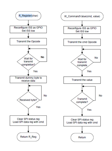
This is the code in the app note for the two functions:

/* ------------------------------------------------------------------
 / Read HI-3110 Register Read Function
 / ------------------------------------------------------------------
 Argument(s): Register to read
 Return: 8-bit Register Value
 */
unsigned char R_Register(char Reg)
{
    unsigned char R_Reg;
    SPI0CR1 = SPI0CR1 & ~SPI0CR1_SSOE_MASK; // disable auto /SS output, reset /SS Output Enable
    SPI0CR2 = SPI0CR2 & ~SPI0CR2_MODFEN_MASK; // disable auto /SS output, reset SPI0 Mode Fault
    SPI0_nSS = 0; // assert the SPI0 /SS strobe
    R_Reg = txrx8bits(Reg, 1); // send op code (ignore returned data byte)
    R_Reg = txrx8bits(0x00, 1); // send dummy data / receive Status Reg byte
    SPI0_nSS = 1; // negate the SPI0 /SS strobe
    SPI0CR1 = SPI0CR1 | SPI0CR1_SSOE_MASK; // enable auto /SS output, set /SS Output Enable
    SPI0CR2 = SPI0CR2 | SPI0CR2_MODFEN_MASK; // enable auto /SS output, set SPI0 Mode Fault
    return R_Reg;
}

// Write SPI Command with a Value to HI-3593
void W_CommandValue(uint8 cmd, uint8 value)
{
    uint8 dummy;
    SPI0CR1 = SPI0CR1 & ~SPI0CR1_SSOE_MASK; // disable auto /SS output, reset /SS Output
    SPI0CR2 = SPI0CR2 & ~SPI0CR2_MODFEN_MASK; // disable auto /SS output, reset SPI0 Mode
    SPI0_nSS = 0; // assert the SPI0 /SS strobe
    dummy = SPI0SR; // clear SPI status register
    SPI0DR = cmd; // SPI command
    while (!SPI0SR_SPIF)
        ;
    dummy = SPI0DR; // read Rx data in Data Reg to reset SPIF
    dummy = SPI0SR; // clear SPI status register
    SPI0DR = value; // Reset values
    while (!SPI0SR_SPIF)
        ;
    dummy = SPI0DR; // read Rx data in Data Reg to reset SPIF
    SPI0_nSS = 1; // negate the SPI0 /SS strobe
    SPI0CR1 = SPI0CR1 | SPI0CR1_SSOE_MASK; // enable auto /SS output, set /SS Output Enable
    SPI0CR2 = SPI0CR2 | SPI0CR2_MODFEN_MASK; // enable auto /SS output, set SPI0 Mode Default
}

And these are my equivallent functions:

void W_CommandValue(uint16_t cmd, uint16_t value)
{
    //Pull the cs pin to low.
    GPIO_writePin(SPIA_CS_PIN, 0);
    //Wait for 100 us.
    DEVICE_DELAY_US(100);
    //Read the dummy data.
    SPI_readDataNonBlocking(A429_SPI);
    //Wait for 100 us.
    DEVICE_DELAY_US(100);
    //Write the command.
    SPI_writeDataNonBlocking(A429_SPI, cmd);
    //Wait for 100 us.
    DEVICE_DELAY_US(100);
    //Read the dummy data.
    SPI_readDataNonBlocking(A429_SPI);
    //Wait for 100 us.
    DEVICE_DELAY_US(100);
    //Write the value.
    SPI_writeDataNonBlocking(A429_SPI, value);
    //wait 100 us.
    DEVICE_DELAY_US(100);
    //Read the dummy data.
    SPI_readDataNonBlocking(A429_SPI);
    //wait 100 us.
    DEVICE_DELAY_US(100);
    //Pull the cs pin to high.
    GPIO_writePin(SPIA_CS_PIN, 1);
    //wait 100 us.
    DEVICE_DELAY_US(100);
}

uint16_t R_Register(uint16_t cmd)
{
    uint16_t value = 0;
    //Pull the cs pin to low.
    GPIO_writePin(SPIA_CS_PIN, 0);
    //Wait for 100 us.
    DEVICE_DELAY_US(100);
    //Write the command.
    SPI_writeDataNonBlocking(A429_SPI, cmd);
    //Wait for 100 us.
    DEVICE_DELAY_US(100);
    //Read the dummy byte.
    SPI_readDataNonBlocking(A429_SPI);
    //Wait for 100 us.
    DEVICE_DELAY_US(100);
    //Transmit dummy data.z
    SPI_writeDataNonBlocking(A429_SPI, 0x00);
    //Wait for 100 us.
    DEVICE_DELAY_US(100);
    //Read the received byte.
    value = SPI_readDataNonBlocking(A429_SPI);
    //Wait for 100 us.
    DEVICE_DELAY_US(100);
    //Pull the cs pin to high.
    GPIO_writePin(SPIA_CS_PIN, 1);
    return value;
}

But i am not able to communicate properly.

I tested the two functions like this:

void initHI3593()
{
//Give raising edge to HI-3593 to do a hardware reset.
GPIO_writePin(A429_CA_RESET, 0);
DEVICE_DELAY_US(100);
GPIO_writePin(A429_CA_RESET, 1);

//Write to ACLK Division Register(0x1400)
DEVICE_DELAY_US(100);
W_CommandValue(0x3800, 0x1400);
DEVICE_DELAY_US(100);
testVar = R_Register(0xD400);
}

The value of testVar should be 0x14, but i get 0x00.

Any sugesstions as to what is going wrong?

  • AK,

    To clarify, what operating mode is the F28377D in? I noticed you have the device reading and writing to the HI-3593, but not vice versa.

    If you haven't already, refer to SPI sections 18.3.1 (Introduction to Operation), 18.3.10 (SPI 3-Wire Mode Description), and 18.4.5 (SPI 3-Wire Mode Code Examples) which I have linked here for your reference. There is specific instructions and example code on how to configure the device and the specific registers to send/receive dummy data. Including this information in your code should help you to see the testVar data.

    Regards,

    Aishwarya

  • Hi Aishwarya,

    I am am operating in Mode 0 as entioned in the HI-3593's datasheet and SPI is clocked at 5Mhz.

    This is my SPI bus configuration:

    //
    // Setup SPI for A429
    //
    void HAL_setupSPI_A429(uint32_t base)
    {
        //GPIO Configuration
            // GPIO58->SPISIMOA->A429_C1_SI
        GPIO_setMasterCore(58, GPIO_CORE_CPU1);
        GPIO_setPinConfig(GPIO_58_SPISIMOA);
        GPIO_setDirectionMode(58, GPIO_DIR_MODE_OUT);
        GPIO_setPadConfig(58, GPIO_PIN_TYPE_STD);
        GPIO_writePin(58,0);
    
        // GPIO59->SPISOMIA->A429_C1_CO
        GPIO_setMasterCore(59, GPIO_CORE_CPU1);
        GPIO_setPinConfig(GPIO_59_SPISOMIA);
        GPIO_setDirectionMode(59, GPIO_DIR_MODE_IN);
        GPIO_setPadConfig(59, GPIO_PIN_TYPE_STD);
    
        // GPIO60->SPICLKA->A429_C1_SCK
        GPIO_setMasterCore(60, GPIO_CORE_CPU1);
        GPIO_setPinConfig(GPIO_60_SPICLKA);
        GPIO_setDirectionMode(60, GPIO_DIR_MODE_OUT);
        GPIO_setPadConfig(60, GPIO_PIN_TYPE_STD);
        GPIO_writePin(60,0);
    
        // GPIO61->SPISTEA->A429_C1_CSn
        GPIO_setMasterCore(61, GPIO_CORE_CPU1);
    //    GPIO_setPinConfig(GPIO_61_SPISTEA);
        GPIO_setPinConfig(GPIO_61_GPIO61);
        GPIO_setDirectionMode(61, GPIO_DIR_MODE_OUT);
        GPIO_setPadConfig(61, GPIO_PIN_TYPE_STD);
        GPIO_writePin(61,0);
    
        //
        // Must put SPI into reset before configuring it
        //
        SPI_disableModule(base);
        //
        // SPI configuration.
        //
        SPI_setConfig(base, DEVICE_LSPCLK_FREQ, SPI_PROT_POL0PHA0,
                      SPI_MODE_MASTER, 500000, 8);
        //
        // FIFO and interrupt configuration
        //
        SPI_disableFIFO(base);
        SPI_clearInterruptStatus(base, SPI_INT_RX_DATA_TX_EMPTY);
        SPI_disableInterrupt(base, SPI_INT_RX_DATA_TX_EMPTY);
        SPI_disableLoopback(base);
        SPI_setEmulationMode(base, SPI_EMULATION_STOP_AFTER_TRANSMIT);
        //
        // Configuration complete. Enable the module.
        //
        SPI_enableModule(base);
        return;
    }

    I was able to communicate with HI-3593, i though i could get away with using Non blocking SPI read/writes, but the timimgs are quiet strict.

    I started using Blocking calls and got some success.

    This is what i have done:

    void W_CommandValue(uint16_t cmd, uint16_t value)
    {
        //Pull the cs pin to low.
        GPIO_writePin(SPIA_CS_PIN, 0);
        //Wait for 100 us.
        DEVICE_DELAY_US(100);
        SPI_writeDataBlockingNonFIFO(A429_SPI, cmd);    //transmit the opcode
        SPI_writeDataBlockingNonFIFO(A429_SPI, value);  //transmit the value
        //wait 100 us.
        DEVICE_DELAY_US(100);
        //Pull the cs pin to high.
        GPIO_writePin(SPIA_CS_PIN, 1);
        //wait 100 us.
        DEVICE_DELAY_US(100);
    }
    
    uint16_t R_Register(uint16_t cmd)
    {
        uint16_t value = 0;
        //Pull the cs pin to low.
        GPIO_writePin(SPIA_CS_PIN, 0);
        //Wait for 100 us.
        DEVICE_DELAY_US(100);
        SPI_writeDataBlockingNonFIFO(A429_SPI, cmd);        //Send opcode
        SPI_writeDataBlockingNonFIFO(A429_SPI, 0x1000);     //Send 0x10 as dummy data
        value = SPI_readDataBlockingNonFIFO(A429_SPI);      //Read received byte
        //Wait for 100 us.
        DEVICE_DELAY_US(100);
        //Pull the cs pin to high.
        GPIO_writePin(SPIA_CS_PIN, 1);
    
        return value;
    }
    
    void initHI3593()
    {
        //Give raising edge to HI-3593 to do a hardware reset.
        GPIO_writePin(A429_CA_RESET, 0);
        DEVICE_DELAY_US(100);
        GPIO_writePin(A429_CA_RESET, 1);
    
        //Write to ACLK Division Register(send 0xD4 and read back 0x14)
        DEVICE_DELAY_US(100);
        W_CommandValue(0x3800, 0x1400);
        DEVICE_DELAY_US(100);
        testVar4 = R_Register(0xD400);
    }


    As of now ,I am controliing the chip select manually as suggestly in the application note:

    Could you suggest the correct way to send/receive multiple bytes.

    I was looking at the C2000ware library and not sure which function does this in spi.h header.

  • AK,

    These functions can transmit/receive 2-4 bytes of data: SPI_transmitByte and SPI_receive16Bits, SPI_transmit24Bits and SPI_receive24Bits, and SPI_transmit32Bits and SPI_transmit32Bits, but they use SPI polling.

    Alternatively, you can use a simple for loop to go through how many ever bits of data you want to transmit/receive within your written function. We do not have an exact example for F28377D, so I've attached a screenshot of an external loopback example for the F2838x device that does a similar thing to what you're trying to do. 

    Other things to consider: check your GPIO pins, clock polarity, and clock phase, and ensure they everything is in sync.

    //#############################################################################
    //
    // FILE:   spi_ex3_external_loopback.c
    //
    // TITLE:  SPI Digital Loopback without using FIFOs and Interrupts
    //
    //! \addtogroup driver_example_list
    //! <h1>SPI Digital External Loopback without FIFO Interrupts</h1>
    //!
    //! This program uses the external loopback between two SPI modules. Both
    //! the SPI FIFOs and interrupts are not used in this example. SPIA is
    //! configured as a peripheral and SPI B is configured as controller. This example
    //! demonstrates full duplex communication where both controller and peripheral transmits
    //! and receives data simultaneously.
    //!
    //!
    //! \b External \b Connections \n
    //!  -GPIO24 and GPIO16 - SPIPICO
    //!  -GPIO25 and GPIO17 - SPIPOCI
    //!  -GPIO26 and GPIO18 - SPICLK
    //!  -GPIO27 and GPIO19 - SPIPTE
    //!
    //! \b Watch \b Variables \n
    //!  - \b TxData_SPIA - Data send from SPIA (peripheral)
    //!  - \b TxData_SPIB - Data send from SPIB (controller)
    //!  - \b RxData_SPIA - Data received by SPIA (peripheral)
    //!  - \b RxData_SPIB - Data received by SPIB (controller)
    //!
    //
    //#############################################################################
    // $Copyright:  $
    //###########################################################################
    
    //
    // Included Files
    //
    #include "driverlib.h"
    #include "device.h"
    #include "board.h"
    
    //
    // Main
    //
    void main(void)
    {
        uint16_t i;
    
        uint16_t TxData_SPIA[] = {0x00, 0x01, 0x02, 0x03, 0x04, 0x05, 0x06, 0x07, 0x08, 0x09, 0x0A, 0x0B, 0x0C, 0x0D, 0x0E, 0x0F};
        uint16_t RxData_SPIA[] = {0x00, 0x00, 0x00, 0x00, 0x00, 0x00, 0x00, 0x00, 0x00, 0x00, 0x00, 0x00, 0x00, 0x00, 0x00, 0x00};
    
        uint16_t TxData_SPIB[] = {0x10, 0x11, 0x12, 0x13, 0x14, 0x15, 0x16, 0x17, 0x18, 0x19, 0x1A, 0x1B, 0x1C, 0x1D, 0x1E, 0x1F};
        uint16_t RxData_SPIB[] = {0x00, 0x00, 0x00, 0x00, 0x00, 0x00, 0x00, 0x00, 0x00, 0x00, 0x00, 0x00, 0x00, 0x00, 0x00, 0x00};
    
        //
        // Initialize device clock and peripherals
        //
        Device_init();
    
        //
        // Disable pin locks and enable internal pullups.
        //
        Device_initGPIO();
    
        //
        // Initialize PIE and clear PIE registers. Disables CPU interrupts.
        //
        Interrupt_initModule();
    
        //
        // Initialize the PIE vector table with pointers to the shell Interrupt
        // Service Routines (ISR).
        //
        Interrupt_initVectorTable();
    
        //
        // Board initialization
        //
        Board_init();
    
        //
        // Loop forever. Suspend or place breakpoints to observe the buffers.
        //
        for(i = 0; i < 16; i++)
        {
            //
            // Set the TX buffer of peripheral SPI.
            //
            SPI_writeDataNonBlocking(SPIA_BASE, TxData_SPIA[i]);
    
            //
            // Set the the controller TX buffer. This triggers the data transmission
            //
            SPI_writeDataNonBlocking(SPIB_BASE, TxData_SPIB[i]);
    
            //
            // Read the received data
            //
            RxData_SPIA[i] = SPI_readDataBlockingNonFIFO(SPIA_BASE);
            RxData_SPIB[i] = SPI_readDataBlockingNonFIFO(SPIB_BASE);
    
            //
            // Check the received data
            //
            if(RxData_SPIA[i] != TxData_SPIB[i])
            {
                ESTOP0;
            }
            if(RxData_SPIB[i] != TxData_SPIA[i])
            {
                ESTOP0;
            }
        }
    
        //
        // Loop forever
        //
        while(1);
    }
    

    Regards,

    Aishwarya

  • Hi Aishwarya,

    Thanks for the detailed reply, One more quiry i need it cleared from you , The TRM manual says that SPI data into the SPITXBuf register is left justified, so if the SPI bus is configured in 8 bit mode , if i want to send 0x01 for example , i need to shift it by 8 and then send (0x0100).

    Should the same be done manually when using  SPI_transmitByte and SPI_receive16Bits, SPI_transmit24Bits and SPI_receive24Bits, and SPI_transmit32Bits and SPI_transmit32Bits?

  • AK,

    Since the SPI registers SPITXBUF and SPIDAT are 16 bits long, you should not have to do the same for 16/24/32 bits operations, but just be mindful of how many bytes are being sent and stored in total.

    Note, that the received data will always be aligned properly since it is shifted into the LSB of SPIDAT.