This thread has been locked.

If you have a related question, please click the "Ask a related question" button in the top right corner. The newly created question will be automatically linked to this question.

TMS320F28379D: Clarity regarding the SOCFRC bit in ADC for Start of Conversion

Part Number: TMS320F28379D

Hello,

I have an application which initializes the ADC A and B and maps some channels to corresponding SOCs. As I am new to this DSP, I needed some clarity on the same.

1. Physically or in hardware, are there 4 ADC modules namely A,B,C,D each having 16 channels? (as per the technical reference manual, there are 4 I have noticed. Wanted to verify if there are 4 different hardware circuits or some form of muxing is present in between them to share the same 16 channels.)

2. If there are multiple ADC modules, do each of these modules have 16 SOCs or there are only 16 SOC circuitry being shared by all 4 modules? The Adc a,b,c,d registers are having different base addresses, I understand.  

3. I have initialised the SOCFRC bit and set it to 1 for all SOCs in my initialization of ADCs file. I am a bit confused regarding how will it be cleared. The reason being, I am using ADCINT1 for triggering my conversion start. But the first start of conversion needs to be started by software forcing and once it starts as and when my conversion gets completed, the ADCINT1 will be triggered and again the conversion will start from SOC0. So the need for SOCFRC to be set 1 is one time. I am not clearing the SOCFRC bit anywhere in my code, so is it cleared by hardware somehow after one time use? 

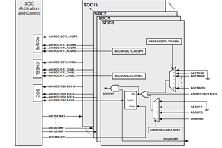
In the diagram shown, there are 3 sources of triggering the SOC, the SOCFRC, the ADCINT and some PWM triggers. My doubt is if SOCFRC is not cleared after the first time, then we donot need to wait for ADCINT to start the 2nd cycle of conversion again (which is desirable in my case as I need to start the 2nd cycle of conversion only after all the SOCs in my 1st cycle has been completed). As it is an OR gate before so any bit in the input, if high, will trigger an output high and hence SOC will begin. So the SOCFRC must be cleared somehow, so as to ensure that my ADCINT1 only triggers the 2nd cycle of SOC. \

It will be very helpful if you could clarify the above issues.

Thanks and Regards,

Prarambhik

  • Hello Prarambhik,

    1. Physically or in hardware, are there 4 ADC modules namely A,B,C,D each having 16 channels? (as per the technical reference manual, there are 4 I have noticed. Wanted to verify if there are 4 different hardware circuits or some form of muxing is present in between them to share the same 16 channels.)

    There are four distinct ADC modules, and each has its own 16-channel input mux. There is also an analog interconnect that links the ADC inputs to the external pins, so you will notice that ADC input pins are also shared with CMPSS inputs. On this device, two of the ADC input pins are shared across all ADC modules - ADCIN14 and ADCIN15.

    2. If there are multiple ADC modules, do each of these modules have 16 SOCs or there are only 16 SOC circuitry being shared by all 4 modules? The Adc a,b,c,d registers are having different base addresses, I understand.  

    Each ADC module has 16 SOC blocks of its own.

    3. I have initialised the SOCFRC bit and set it to 1 for all SOCs in my initialization of ADCs file. I am a bit confused regarding how will it be cleared. The reason being, I am using ADCINT1 for triggering my conversion start. But the first start of conversion needs to be started by software forcing and once it starts as and when my conversion gets completed, the ADCINT1 will be triggered and again the conversion will start from SOC0. So the need for SOCFRC to be set 1 is one time. I am not clearing the SOCFRC bit anywhere in my code, so is it cleared by hardware somehow after one time use? 

    The ADCSOCFRC register is not meant to be initialized; that is the register that you write to when you want to trigger a conversion start using software. First you must configure ADCSOCxCTL to configure the sample window, channel selection and trigger source. Then you write 1 to the desired SOC bit in ADCSOCFRC to force a software conversion. Reads of this register will always return 0. ADCINTx is the ADC interrupt signal that gets set at the end of conversion (or at the end of the sample+hold phase/start of conversion phase if ADCCTL1.INTPULSEPOS = 0).

    Using ADCINTx to trigger a conversion is intended for when you want one SOC to begin immediately after another ends. In this case, you configure ADCINTSOCSEL1/2 to specify which ADCINT will trigger the desired SOC. The ADCINT itself must be associated with the end of a particular SOC by writing to ADCINTSEL1N2.

    For more details, please see the ADC chapter of the device TRM.

    Best regards,
    Ibukun

  • Hello Ibukun,

    Thanks for the clarification. This resolved my doubts.

    Regards,

    Prarambhik