This thread has been locked.

If you have a related question, please click the "Ask a related question" button in the top right corner. The newly created question will be automatically linked to this question.

TMS320F280039C: PWM spike problem when dead band submodule is enabled/disabled

Part Number: TMS320F280039C
Other Parts Discussed in Thread: TMDSCNCD280039C, TMDSHSECDOCK

Dear Texas Instruments Team,

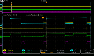
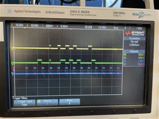
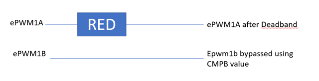
 At the moment, I am developing the software to control the LLC converter. As you already know during the startup asymmetrical PWM is required for a first few PWM cycles, and later the symmetrical complementary PWM mode is needed. In the attached Figure, first 6 PWM cycles shows an example for PWM pattern during the startup procedure for LLC.

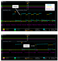
Figure 1: PWM pattern for startup procedure.

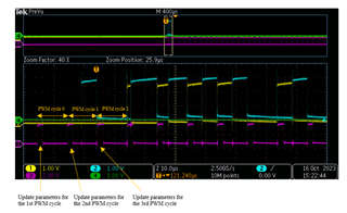
Here are some notes for first six PWM patterns:

1st PWM cycle – only low side MOSFET shall be turned on. High side MOSFET is turned off. PWM is not working in complementary mode.

2nd PWM cycle – both, low side and high side MOSFETs shall be turned off. PWM is not working in complementary mode.

3rd PWM cycle – low side and high side MOSFET operate at complementary mode where duty cycle for high-side MOSFET is smaller compared to the low side MOSFET.

4th PWM cycle - low side and high side MOSFET operate at complementary mode where duty cycle for high-side MOSFET is smaller compared to the low side MOSFET, but the ration between low side and high side duty cycle is now changed. Duty cycle for high side MOSFET is increased and duty cycle for low side is decreased.

5th PWM cycle - low side and high side MOSFET operate at complementary mode with the symmetrical PWM pattern – duty cycle for both PWM signals is 50 %.

6th PWM cycle - low side and high side MOSFET operate at complementary mode with the symmetrical PWM pattern – duty cycle for both PWM signals is 50 %.

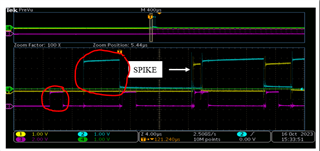
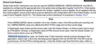
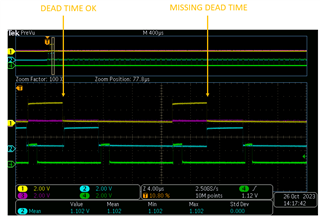
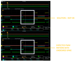
I attached the main.c file used to test the startup PWM pattern. Inside the PWM interrupt, the PWM parameters are updated for every new PWM cycle. To make everything transparent and synchronous, the global load option is selected to update all the required registers at the same time. The problem which occurs is with the start of 3rd PWM cycle where smaller spike occurs at the start of the PWM cycle. This is not spike caused by the interference or neither it is introduced by the bad measurement setup. My assumption is that it happens because the Dead Band Submodule is bypassed in 2nd PWM cycle and in the 3rd PWM cycle is enabled. But I do not understand why because the global load is enabled. Can you please tell me why is this happening and how to solve an issue with the spike. This behaviour is not acceptable.

/******************************************************************************/
/* COPYRIGHT (c) 2023                                                         */
/* AEconversion                                                               */
/* All rights reserved.                                                       */
/******************************************************************************/
/*!
* @file     main.c
* @author   Haris Kovacevic
* @date     September 19, 2023
* @brief    Main function
* @version  V1.0.0
*/
/******************************************************************************/
/*!
 * @addtogroup MAIN
 * @{ <!-- BEGIN GROUP -->
 */
/******************************************************************************/

/******************************************************************************/
/* Includes                                                                   */
/******************************************************************************/
#include "device.h"
#include "interrupt.h"
#include "sw_interrupt_prioritization_logic.h"

/******************************************************************************/
/* Definitions                                                                */
/******************************************************************************/


/******************************************************************************/
/* Typedefs                                                                   */
/******************************************************************************/


/******************************************************************************/
/* Variables                                                                  */
/******************************************************************************/
extern uint16_t RamfuncsLoadStart;
extern uint16_t RamfuncsLoadEnd;
extern uint16_t RamfuncsLoadSize;
extern uint16_t RamfuncsRunStart;
extern uint16_t RamfuncsRunEnd;
extern uint16_t RamfuncsRunSize;
extern uint16_t Cla1ProgLoadStart;
extern uint16_t Cla1ProgRunStart;
extern uint16_t Cla1ProgLoadSize;

volatile uint32_t cnt_test = 0UL;

/******************************************************************************/
/* Function prototypes                                                        */
/******************************************************************************/
__interrupt void    pwm1_isr        (void);
static void         flash_init      (void);
static void         cpu_init        (void);
static void         gpio_init       (void);
static void         pwm_init        (void);

/******************************************************************************/
/* Functions                                                                  */
/******************************************************************************/

/******************************************************************************/
/*
 * MAIN FUNCTION
 */
/******************************************************************************/
void main(void)
{
    /* Copy time critical code and flash setup code to RAM.
     * The RamfuncsLoadStart, RamfuncsLoadSize, RamfuncsRunStart, Cla1ProgRunStart,
     * Cla1ProgLoadStart, and Cla1ProgLoadSize are created by the linker.
     * Refer to the device .cmd file. */
    memcpy((uint32_t *)&RamfuncsRunStart, (uint32_t *)&RamfuncsLoadStart,
           (uint32_t)&RamfuncsLoadSize );
    memcpy((uint32_t *)&Cla1ProgRunStart, (uint32_t *)&Cla1ProgLoadStart,
           (uint32_t)&Cla1ProgLoadSize );

    /* Initialize PIE and clear PIE registers. Disables CPU interrupts. */
    Interrupt_initModule();

    /* Initialize the PIE vector table with pointers to the shell Interrupt
       Service Routines (ISR). */
    Interrupt_initVectorTable();

    /* Flash initialization */
    flash_init();
    /* CPU initialization */
    cpu_init();
    /* GPIO initialization */
    gpio_init();
    /* PWM initialization */
    pwm_init();

    /* Enable PWM 1 interrupt */
    Interrupt_enable(INT_EPWM1);

    /* Enable sync and clock to PWM */
    SysCtl_enablePeripheral(SYSCTL_PERIPH_CLK_TBCLKSYNC);

    /* Enable Global Interrupt (INTM) and realtime interrupt (DBGM) */
    EINT;
    ERTM;

    while(1)
    {
        /* Infinite loop */

    }
}

/******************************************************************************/
/*
 * FLASH INITIALIZATION
 */
/******************************************************************************/
static void flash_init(void)
{
    /* Set the bank fallback power modes to active */
    Flash_setBankPowerMode(FLASH0CTRL_BASE, FLASH_BANK0, FLASH_BANK_PWR_ACTIVE);
    Flash_setBankPowerMode(FLASH0CTRL_BASE, FLASH_BANK1, FLASH_BANK_PWR_ACTIVE);
    Flash_setBankPowerMode(FLASH0CTRL_BASE, FLASH_BANK2, FLASH_BANK_PWR_ACTIVE);

    /* Power up flash bank and pump and this also sets the fall back mode of
     * flash and pump as active */
    Flash_setPumpPowerMode(FLASH0CTRL_BASE, FLASH_PUMP_PWR_ACTIVE);

    /* Disable cache and prefetch mechanism before changing wait states */
    Flash_disableCache(FLASH0CTRL_BASE);
    Flash_disablePrefetch(FLASH0CTRL_BASE);

    /* Set waitstates according to frequency */
    Flash_setWaitstates(FLASH0CTRL_BASE, 5);

    /* Enable cache and prefetch mechanism to improve performance of code
     * executed from flash */
    Flash_enableCache(FLASH0CTRL_BASE);
    Flash_enablePrefetch(FLASH0CTRL_BASE);

    /* At reset, ECC is enabled.  If it is disabled by application software and
     * if application again wants to enable ECC. */
    Flash_enableECC(FLASH0ECC_BASE);

    /* Force a pipeline flush to ensure that the write to the last register
     * configured occurs before returning */
    __asm(" RPT #7 || NOP");
}

/******************************************************************************/
/*
 * CPU INITIALIZATION
 */
/******************************************************************************/
static void cpu_init(void)
{
    /* Disable Watchdog */
    SysCtl_disableWatchdog();

    SysCtl_setClock(SYSCTL_OSCSRC_OSC1 |
                    SYSCTL_IMULT(24U) |
                    SYSCTL_REFDIV(2U) |
                    SYSCTL_ODIV(1U) |
                    SYSCTL_SYSDIV(1U) |
                    SYSCTL_PLL_ENABLE);

    /* Set Low speed clock divider */
    SysCtl_setLowSpeedClock(SYSCTL_LSPCLK_PRESCALE_4);

    /* Clock source connected to output pin */
    SysCtl_selectClockOutSource(SYSCTL_CLOCKOUT_SYSCLK);
    SysCtl_setXClk(SYSCTL_XCLKOUT_DIV_1);

    SysCtl_enablePeripheral(SYSCTL_PERIPH_CLK_TIMER0);
    SysCtl_enablePeripheral(SYSCTL_PERIPH_CLK_TIMER1);
    SysCtl_enablePeripheral(SYSCTL_PERIPH_CLK_TIMER2);
    SysCtl_enablePeripheral(SYSCTL_PERIPH_CLK_TBCLKSYNC);
    SysCtl_enablePeripheral(SYSCTL_PERIPH_CLK_EPWM1);
    SysCtl_enablePeripheral(SYSCTL_PERIPH_CLK_EPWM2);
    SysCtl_enablePeripheral(SYSCTL_PERIPH_CLK_EPWM3);
    SysCtl_enablePeripheral(SYSCTL_PERIPH_CLK_EPWM4);
    SysCtl_enablePeripheral(SYSCTL_PERIPH_CLK_EPWM5);
    SysCtl_enablePeripheral(SYSCTL_PERIPH_CLK_EPWM6);
    SysCtl_enablePeripheral(SYSCTL_PERIPH_CLK_EPWM7);
    SysCtl_enablePeripheral(SYSCTL_PERIPH_CLK_EPWM8);
    SysCtl_enablePeripheral(SYSCTL_PERIPH_CLK_HRCAL);
    SysCtl_enablePeripheral(SYSCTL_PERIPH_CLK_SCIA);
    SysCtl_enablePeripheral(SYSCTL_PERIPH_CLK_SCIB);
    SysCtl_enablePeripheral(SYSCTL_PERIPH_CLK_ADCA);
    SysCtl_enablePeripheral(SYSCTL_PERIPH_CLK_ADCB);
    SysCtl_enablePeripheral(SYSCTL_PERIPH_CLK_ADCC);
    SysCtl_enablePeripheral(SYSCTL_PERIPH_CLK_CMPSS1);
    SysCtl_enablePeripheral(SYSCTL_PERIPH_CLK_CMPSS2);
    SysCtl_enablePeripheral(SYSCTL_PERIPH_CLK_CMPSS3);
    SysCtl_enablePeripheral(SYSCTL_PERIPH_CLK_CMPSS4);
    SysCtl_enablePeripheral(SYSCTL_PERIPH_CLK_DACA);
    SysCtl_enablePeripheral(SYSCTL_PERIPH_CLK_DACB);
    SysCtl_enablePeripheral(SYSCTL_PERIPH_CLK_CLB1);
    SysCtl_enablePeripheral(SYSCTL_PERIPH_CLK_CLB2);
    SysCtl_enablePeripheral(SYSCTL_PERIPH_CLK_CLB3);
    SysCtl_enablePeripheral(SYSCTL_PERIPH_CLK_CLB4);
    SysCtl_enablePeripheral(SYSCTL_PERIPH_CLK_CLA1);
    SysCtl_enablePeripheral(SYSCTL_PERIPH_CLK_ECAP1);
    SysCtl_enablePeripheral(SYSCTL_PERIPH_CLK_ECAP2);
    SysCtl_enablePeripheral(SYSCTL_PERIPH_CLK_ECAP3);
    SysCtl_enablePeripheral(SYSCTL_PERIPH_CLK_I2CA);
    SysCtl_enablePeripheral(SYSCTL_PERIPH_CLK_I2CB);
    SysCtl_enablePeripheral(SYSCTL_PERIPH_CLK_SPIA);
    SysCtl_enablePeripheral(SYSCTL_PERIPH_CLK_SPIB);
    SysCtl_enablePeripheral(SYSCTL_PERIPH_CLK_CANA);
    SysCtl_enablePeripheral(SYSCTL_PERIPH_CLK_MCANA);
}

/******************************************************************************/
/*
 * GPIO INITIALIZATION
 */
/******************************************************************************/
static void gpio_init(void)
{
    /* Configure GPIO pin 0 */
    GPIO_setDirectionMode(0, GPIO_DIR_MODE_OUT);
    GPIO_setPadConfig(0, GPIO_PIN_TYPE_STD);
    GPIO_setMasterCore(0, GPIO_CORE_CPU1);
    GPIO_writePin(0, (uint32_t)0);
    GPIO_setPinConfig(GPIO_0_EPWM1_A);

    /* Configure GPIO pin 1 */
    GPIO_setDirectionMode(1, GPIO_DIR_MODE_OUT);
    GPIO_setPadConfig(1, GPIO_PIN_TYPE_STD);
    GPIO_setMasterCore(1, GPIO_CORE_CPU1);
    GPIO_writePin(1, (uint32_t)0);
    GPIO_setPinConfig(GPIO_1_EPWM1_B);

    /* Configure GPIO pin 44 */
    GPIO_setDirectionMode(44, GPIO_DIR_MODE_OUT);
    GPIO_setPadConfig(44, GPIO_PIN_TYPE_STD);
    GPIO_setMasterCore(44, GPIO_CORE_CPU1);
    GPIO_writePin(44, (uint32_t)0);
    GPIO_setPinConfig(GPIO_44_GPIO44);
}

/******************************************************************************/
/*
 * PWM INITIALIZATION
 */
/******************************************************************************/
static void pwm_init(void)
{
    /* Disable sync (Freeze clock to PWM as well) */
    SysCtl_disablePeripheral(SYSCTL_PERIPH_CLK_TBCLKSYNC);

    /* Connect interrupt functions to vector addresses */
    Interrupt_register(INT_EPWM1, &pwm1_isr);

    /* Set PWM counter type and clock dividers */
    EPWM_setTimeBaseCounterMode(EPWM1_BASE, EPWM_COUNTER_MODE_UP);
    EPWM_setTimeBaseCounter(EPWM1_BASE, 0U);
    EPWM_setClockPrescaler(EPWM1_BASE, EPWM_CLOCK_DIVIDER_1, EPWM_HSCLOCK_DIVIDER_1);
    EPWM_setTimeBasePeriod(EPWM1_BASE, 1200U);

    /* Set PWM emulation mode */
    EPWM_setEmulationMode(EPWM1_BASE, EPWM_EMULATION_FREE_RUN);
    /* Phase shift load setup */
    EPWM_disablePhaseShiftLoad(EPWM1_BASE);
    EPWM_setPhaseShift(EPWM1_BASE, 0U);

    /* Set PWM period load configuration */
    EPWM_setPeriodLoadMode(EPWM1_BASE, EPWM_PERIOD_SHADOW_LOAD);
    EPWM_selectPeriodLoadEvent(EPWM1_BASE, EPWM_SHADOW_LOAD_MODE_COUNTER_ZERO);

    /* Set PWM compare register load configuration and initial duty cycle */
    EPWM_setCounterCompareShadowLoadMode(EPWM1_BASE, EPWM_COUNTER_COMPARE_A, EPWM_COMP_LOAD_ON_CNTR_ZERO);
    EPWM_setCounterCompareShadowLoadMode(EPWM1_BASE, EPWM_COUNTER_COMPARE_B, EPWM_COMP_LOAD_ON_CNTR_ZERO);
    EPWM_setCounterCompareShadowLoadMode(EPWM1_BASE, EPWM_COUNTER_COMPARE_C, EPWM_COMP_LOAD_ON_CNTR_ZERO);
    EPWM_setCounterCompareShadowLoadMode(EPWM1_BASE, EPWM_COUNTER_COMPARE_D, EPWM_COMP_LOAD_ON_CNTR_ZERO);

    /* Action qualifier setting */
    EPWM_setActionQualifierAction(EPWM1_BASE, EPWM_AQ_OUTPUT_A, EPWM_AQ_OUTPUT_HIGH, EPWM_AQ_OUTPUT_ON_TIMEBASE_ZERO);
    EPWM_setActionQualifierAction(EPWM1_BASE, EPWM_AQ_OUTPUT_A, EPWM_AQ_OUTPUT_LOW, EPWM_AQ_OUTPUT_ON_TIMEBASE_UP_CMPA);
    EPWM_setActionQualifierAction(EPWM1_BASE, EPWM_AQ_OUTPUT_B, EPWM_AQ_OUTPUT_LOW, EPWM_AQ_OUTPUT_ON_TIMEBASE_ZERO);
    EPWM_setActionQualifierAction(EPWM1_BASE, EPWM_AQ_OUTPUT_B, EPWM_AQ_OUTPUT_HIGH, EPWM_AQ_OUTPUT_ON_TIMEBASE_UP_CMPB);
    EPWM_setActionQualifierT1TriggerSource(EPWM1_BASE, EPWM_AQ_TRIGGER_EVENT_TRIG_TZ_1);
    EPWM_setActionQualifierT2TriggerSource(EPWM1_BASE, EPWM_AQ_TRIGGER_EVENT_TRIG_TZ_1);

    /* Set Dead-Band settings for Complementary Mode */
    HWREGH(EPWM1_BASE + EPWM_O_DBCTL2) = 0x4U;  // All writes and reads to bits [5:0] of the DBCTL register are shadowed
    EPWM_setDeadBandCounterClock(EPWM1_BASE, EPWM_DB_COUNTER_CLOCK_FULL_CYCLE);
    EPWM_setRisingEdgeDeadBandDelayInput(EPWM1_BASE, EPWM_DB_INPUT_EPWMA);
    EPWM_setRisingEdgeDelayCount(EPWM1_BASE, 25U);
    EPWM_setDeadBandDelayPolarity(EPWM1_BASE, EPWM_DB_FED, EPWM_DB_POLARITY_ACTIVE_LOW);
    EPWM_setFallingEdgeDeadBandDelayInput(EPWM1_BASE, EPWM_DB_INPUT_EPWMA);
    EPWM_setFallingEdgeDelayCount(EPWM1_BASE, 25U);
    HWREGH(EPWM1_BASE + EPWM_O_AQCSFRC) = 0x5;  // Force PWM1 A and B to LOW state

    /* Set compare values */
    EPWM_setCounterCompareValue(EPWM1_BASE, EPWM_COUNTER_COMPARE_A, 0U);
    EPWM_setCounterCompareValue(EPWM1_BASE, EPWM_COUNTER_COMPARE_B, 6000U);

    /* Enable PWM1 interrupt */
    EPWM_setInterruptSource(EPWM1_BASE, EPWM_INT_TBCTR_ZERO);
    EPWM_enableInterrupt(EPWM1_BASE);
    EPWM_setInterruptEventCount(EPWM1_BASE, 1U);

    /* Global load configuration */
    EPWM_enableGlobalLoadRegisters(EPWM1_BASE, EPWM_GL_REGISTER_TBPRD_TBPRDHR);
    EPWM_enableGlobalLoadRegisters(EPWM1_BASE, EPWM_GL_REGISTER_CMPA_CMPAHR);
    EPWM_enableGlobalLoadRegisters(EPWM1_BASE, EPWM_GL_REGISTER_CMPB_CMPBHR);
    //EPWM_enableGlobalLoadRegisters(EPWM1_BASE, EPWM_GL_REGISTER_CMPC);
    //EPWM_enableGlobalLoadRegisters(EPWM1_BASE, EPWM_GL_REGISTER_CMPD);
    EPWM_enableGlobalLoadRegisters(EPWM1_BASE, EPWM_GL_REGISTER_DBRED_DBREDHR);
    EPWM_enableGlobalLoadRegisters(EPWM1_BASE, EPWM_GL_REGISTER_DBFED_DBFEDHR);
    EPWM_enableGlobalLoadRegisters(EPWM1_BASE, EPWM_GL_REGISTER_DBCTL);
    EPWM_enableGlobalLoadRegisters(EPWM1_BASE, EPWM_GL_REGISTER_AQCTLA_AQCTLA2);
    EPWM_enableGlobalLoadRegisters(EPWM1_BASE, EPWM_GL_REGISTER_AQCTLB_AQCTLB2);
    EPWM_enableGlobalLoadRegisters(EPWM1_BASE, EPWM_GL_REGISTER_AQCSFRC);

    EPWM_setGlobalLoadEventPrescale(EPWM1_BASE, 1U);
    EPWM_disableGlobalLoadOneShotMode(EPWM1_BASE);
    EPWM_setGlobalLoadTrigger(EPWM1_BASE, /*EPWM_GL_LOAD_PULSE_CNTR_PERIOD*/EPWM_GL_LOAD_PULSE_CNTR_ZERO);
    EPWM_enableGlobalLoad(EPWM1_BASE);
    //EPWM_disableGlobalLoad(EPWM1_BASE);
}

/******************************************************************************/
/*
 * PWM1 ISR
 */
/******************************************************************************/
__interrupt void pwm1_isr(void)
{
    HWREG(GPIODATA_BASE + GPIO_O_GPBSET) = (0x1U << 12U);

    /* Save IER register on stack */
    volatile uint16_t tempPIEIER = HWREGH(PIECTRL_BASE + PIE_O_IER3);

    /* Set the global and group priority to allow CPU interrupts
       with higher priority */
    IER |= M_INT3;
    IER &= MINT3;
    HWREGH(PIECTRL_BASE + PIE_O_IER3) &= MG3_1;

    /* Enable Interrupts */
    Interrupt_clearACKGroup(0xFFFFU);
    __asm("  NOP");
    EINT;


    /* Code to execute inside interrupt */
    switch(cnt_test)
    {
        case 0:

            /******************************** 1st PWM CYCLE ********************************/

#if 0
            /* Update PWM parameters */
            HWREGH(EPWM1_BASE + EPWM_O_TBPRD) = 1200UL;
            HWREGH(EPWM1_BASE + EPWM_O_CMPA + 0U + 0x1U) = 600UL;
            HWREGH(EPWM1_BASE + EPWM_O_CMPB + 0U + 0x1U) = 600UL;
            HWREGH(EPWM1_BASE + EPWM_O_DBRED) = 25UL;
            HWREGH(EPWM1_BASE + EPWM_O_DBFED) = 25UL;

            /* Force PWM1 A and PWM1 B is defined by CMPA register and counter equal to
             * period/zero */
            HWREGH(EPWM1_BASE + EPWM_O_AQCSFRC) = 0x1;
            /* Load on time-base counter equals zero */
            HWREGH(EPWM1_BASE + EPWM_O_AQSFRC) = 0x0/*0xC0*/;
#endif

            /* Update PWM parameters */
            HWREGH(EPWM1_BASE + EPWM_O_TBPRD) = 1200UL;
            HWREGH(EPWM1_BASE + EPWM_O_CMPA + 0U + 0x1U) = 0UL;
            HWREGH(EPWM1_BASE + EPWM_O_CMPB + 0U + 0x1U) = 600UL;
            HWREGH(EPWM1_BASE + EPWM_O_DBRED) = 25UL;
            HWREGH(EPWM1_BASE + EPWM_O_DBFED) = 25UL;

            HWREGH(EPWM1_BASE + EPWM_O_AQCTLA) = 0x0012U;
            HWREGH(EPWM1_BASE + EPWM_O_AQCTLB) = 0x0201U;

            /* Force PWM1 A and PWM1 B is defined by CMPA register and counter equal to
             * period/zero */
            HWREGH(EPWM1_BASE + EPWM_O_AQCSFRC) = 0x0;
            /* Load on time-base counter equals zero */
            HWREGH(EPWM1_BASE + EPWM_O_AQSFRC) = 0x0/*0xC0*/;

            /* All writes and reads to bits[5:0] of the DBCTL registers are shadowed. */
            HWREGH(EPWM1_BASE + EPWM_O_DBCTL2) = 0x4U;
            /* Bypass dead band submodule */
            HWREGH(EPWM1_BASE + EPWM_O_DBCTL) = 0x0C08U;

            cnt_test += 1U;

            /*******************************************************************************/

            break;
        case 1:

            /******************************** 2nd PWM CYCLE ********************************/

#if 0
            /* Update PWM parameters */
            HWREGH(EPWM1_BASE + EPWM_O_TBPRD) = 1200UL;
            HWREGH(EPWM1_BASE + EPWM_O_CMPA + 0U + 0x1U) = 600UL;
            HWREGH(EPWM1_BASE + EPWM_O_CMPB + 0U + 0x1U) = 600UL;
            HWREGH(EPWM1_BASE + EPWM_O_DBRED) = 25UL;
            HWREGH(EPWM1_BASE + EPWM_O_DBFED) = 25UL;

            /* Load on time-base counter equals zero */
            HWREGH(EPWM1_BASE + EPWM_O_AQSFRC) = 0x0;
            /* Force PWM1 A and B to LOW state */
            HWREGH(EPWM1_BASE + EPWM_O_AQCSFRC) = 0x5;
#endif

            /* Update PWM parameters */
            HWREGH(EPWM1_BASE + EPWM_O_TBPRD) = 1200UL;
            HWREGH(EPWM1_BASE + EPWM_O_CMPA + 0U + 0x1U) = 0UL;
            HWREGH(EPWM1_BASE + EPWM_O_CMPB + 0U + 0x1U) = 0UL;
            HWREGH(EPWM1_BASE + EPWM_O_DBRED) = 25UL;
            HWREGH(EPWM1_BASE + EPWM_O_DBFED) = 25UL;

            HWREGH(EPWM1_BASE + EPWM_O_AQCTLA) = 0x0012U;
            HWREGH(EPWM1_BASE + EPWM_O_AQCTLB) = 0x0102U;

            /* Force PWM1 A and PWM1 B is defined by CMPA register and counter equal to
             * period/zero */
            HWREGH(EPWM1_BASE + EPWM_O_AQCSFRC) = 0x0;
            /* Load on time-base counter equals zero */
            HWREGH(EPWM1_BASE + EPWM_O_AQSFRC) = 0x0/*0xC0*/;

            /* All writes and reads to bits[5:0] of the DBCTL registers are shadowed. */
            HWREGH(EPWM1_BASE + EPWM_O_DBCTL2) = 0x4U;
            /* Bypass dead band submodule */
            HWREGH(EPWM1_BASE + EPWM_O_DBCTL) = 0x0C08U;

            cnt_test += 1U;

            /*******************************************************************************/

            break;
        case 2:

            /******************************** 3rd PWM CYCLE ********************************/

#if 0
            /* Update PWM parameters */
            HWREGH(EPWM1_BASE + EPWM_O_TBPRD) = 1200UL;
            HWREGH(EPWM1_BASE + EPWM_O_CMPA + 0U + 0x1U) = 150UL;
            HWREGH(EPWM1_BASE + EPWM_O_CMPB + 0U + 0x1U) = 150UL;
            HWREGH(EPWM1_BASE + EPWM_O_DBRED) = 25UL;
            HWREGH(EPWM1_BASE + EPWM_O_DBFED) = 25UL;

            /* Load on time-base counter equals zero */
            HWREGH(EPWM1_BASE + EPWM_O_AQSFRC) = 0x0;
            /* Forcing for PWM1 A and B is disabled */
            HWREGH(EPWM1_BASE + EPWM_O_AQCSFRC) = 0x0;
#endif

            /* Update PWM parameters */
            HWREGH(EPWM1_BASE + EPWM_O_TBPRD) = 1200UL;
            HWREGH(EPWM1_BASE + EPWM_O_CMPA + 0U + 0x1U) = 150UL;
            HWREGH(EPWM1_BASE + EPWM_O_CMPB + 0U + 0x1U) = 150UL;
            HWREGH(EPWM1_BASE + EPWM_O_DBRED) = 25UL;
            HWREGH(EPWM1_BASE + EPWM_O_DBFED) = 25UL;

            HWREGH(EPWM1_BASE + EPWM_O_AQCTLA) = 0x0012U;
            HWREGH(EPWM1_BASE + EPWM_O_AQCTLB) = 0x0102U;

            /* All writes and reads to bits[5:0] of the DBCTL registers are shadowed. */
            HWREGH(EPWM1_BASE + EPWM_O_DBCTL2) = /*0x4U*/0x4U;
            /* Bypass dead band submodule */
            HWREGH(EPWM1_BASE + EPWM_O_DBCTL) = 0x0C0B/*0x0C0A*//*0x0C09*/;

            cnt_test += 1U;

            /*******************************************************************************/

            break;

        case 3:

            /******************************** 4th PWM CYCLE ********************************/

            /* Update PWM parameters */
            HWREGH(EPWM1_BASE + EPWM_O_TBPRD) = 1200UL;
            HWREGH(EPWM1_BASE + EPWM_O_CMPA + 0U + 0x1U) = 450UL;
            HWREGH(EPWM1_BASE + EPWM_O_CMPB + 0U + 0x1U) = 450UL;
            HWREGH(EPWM1_BASE + EPWM_O_DBRED) = 25UL;
            HWREGH(EPWM1_BASE + EPWM_O_DBFED) = 25UL;

            /* Load on time-base counter equals zero */
            HWREGH(EPWM1_BASE + EPWM_O_AQSFRC) = 0x0;
            /* Forcing for PWM1 A and B is disabled */
            HWREGH(EPWM1_BASE + EPWM_O_AQCSFRC) = 0x0;

            /* All writes and reads to bits[5:0] of the DBCTL registers are shadowed. */
            HWREGH(EPWM1_BASE + EPWM_O_DBCTL2) = /*0x4U*/0x4U;
            /* Bypass dead band submodule */
            HWREGH(EPWM1_BASE + EPWM_O_DBCTL) = 0x0C0B;

            cnt_test += 1U;

            /*******************************************************************************/

            break;

        case 4:

            /******************************** 5th PWM CYCLE ********************************/

            /* Update PWM parameters */
            HWREGH(EPWM1_BASE + EPWM_O_TBPRD) = 1200UL;
            HWREGH(EPWM1_BASE + EPWM_O_CMPA + 0U + 0x1U) = 600UL;
            HWREGH(EPWM1_BASE + EPWM_O_CMPB + 0U + 0x1U) = 600UL;
            HWREGH(EPWM1_BASE + EPWM_O_DBRED) = 25UL;
            HWREGH(EPWM1_BASE + EPWM_O_DBFED) = 25UL;

            /* Load on time-base counter equals zero */
            HWREGH(EPWM1_BASE + EPWM_O_AQSFRC) = 0x0;
            /* Forcing for PWM1 A and B is disabled */
            HWREGH(EPWM1_BASE + EPWM_O_AQCSFRC) = 0x0;

            /* All writes and reads to bits[5:0] of the DBCTL registers are shadowed. */
            HWREGH(EPWM1_BASE + EPWM_O_DBCTL2) = /*0x4U*/0x4U;
            /* Bypass dead band submodule */
            HWREGH(EPWM1_BASE + EPWM_O_DBCTL) = 0x0C0B;

            cnt_test += 1U;

            /*******************************************************************************/

            break;

        case 5:

            /******************************** 6th PWM CYCLE ********************************/

            /* Update PWM parameters */
            HWREGH(EPWM1_BASE + EPWM_O_TBPRD) = 1200UL;
            HWREGH(EPWM1_BASE + EPWM_O_CMPA + 0U + 0x1U) = 600UL;
            HWREGH(EPWM1_BASE + EPWM_O_CMPB + 0U + 0x1U) = 600UL;
            HWREGH(EPWM1_BASE + EPWM_O_DBRED) = 25UL;
            HWREGH(EPWM1_BASE + EPWM_O_DBFED) = 25UL;

            /* All writes and reads to bits[5:0] of the DBCTL registers are shadowed. */
            HWREGH(EPWM1_BASE + EPWM_O_DBCTL2) = 0x4U;
            /* Bypass dead band submodule */
            HWREGH(EPWM1_BASE + EPWM_O_DBCTL) = 0x0C0B;

            /* Load on time-base counter equals zero */
            HWREGH(EPWM1_BASE + EPWM_O_AQSFRC) = 0x0;
            /* Force PWM1 A and B to LOW state */
            HWREGH(EPWM1_BASE + EPWM_O_AQCSFRC) = 0x0;

            cnt_test += 1U;

            /*******************************************************************************/
            break;

        case 6:

            /******************************** 7th PWM CYCLE ********************************/

            /* Update PWM parameters */
            HWREGH(EPWM1_BASE + EPWM_O_TBPRD) = 1200UL;
            HWREGH(EPWM1_BASE + EPWM_O_CMPA + 0U + 0x1U) = 600UL;
            HWREGH(EPWM1_BASE + EPWM_O_CMPB + 0U + 0x1U) = 600UL;
            HWREGH(EPWM1_BASE + EPWM_O_DBRED) = 25UL;
            HWREGH(EPWM1_BASE + EPWM_O_DBFED) = 25UL;

            /* Load on time-base counter equals zero */
            HWREGH(EPWM1_BASE + EPWM_O_AQSFRC) = 0x0;
            /* Force PWM1 A and B to LOW state */
            HWREGH(EPWM1_BASE + EPWM_O_AQCSFRC) = 0x5;

            /* All writes and reads to bits[5:0] of the DBCTL registers are shadowed. */
            HWREGH(EPWM1_BASE + EPWM_O_DBCTL2) = 0x4U;
            /* Bypass dead band submodule */
            HWREGH(EPWM1_BASE + EPWM_O_DBCTL) = 0x0C08/*0x0C0A*/;

            cnt_test += 1U;

            /*******************************************************************************/

            break;

        case 7:

            /******************************** 8th PWM CYCLE ********************************/

            /* Update PWM parameters */
            HWREGH(EPWM1_BASE + EPWM_O_TBPRD) = 1200UL;
            HWREGH(EPWM1_BASE + EPWM_O_CMPA + 0U + 0x1U) = 600UL;
            HWREGH(EPWM1_BASE + EPWM_O_CMPB + 0U + 0x1U) = 600UL;
            HWREGH(EPWM1_BASE + EPWM_O_DBRED) = 25UL;
            HWREGH(EPWM1_BASE + EPWM_O_DBFED) = 25UL;

            /* Load on time-base counter equals zero */
            HWREGH(EPWM1_BASE + EPWM_O_AQSFRC) = 0x0;
            /* Force PWM1 A and B to LOW state */
            HWREGH(EPWM1_BASE + EPWM_O_AQCSFRC) = 0x0;

            /* All writes and reads to bits[5:0] of the DBCTL registers are shadowed. */
            HWREGH(EPWM1_BASE + EPWM_O_DBCTL2) = 0x4U;
            /* Bypass dead band submodule */
            HWREGH(EPWM1_BASE + EPWM_O_DBCTL) = /*0x0C0B*/0x0C09;

            cnt_test += 1U;

            /*******************************************************************************/

            break;

        case 8:

            /******************************** 9th PWM CYCLE ********************************/

            /* Update PWM parameters */
            HWREGH(EPWM1_BASE + EPWM_O_TBPRD) = 1200UL;
            HWREGH(EPWM1_BASE + EPWM_O_CMPA + 0U + 0x1U) = 600UL;
            HWREGH(EPWM1_BASE + EPWM_O_CMPB + 0U + 0x1U) = 600UL;
            HWREGH(EPWM1_BASE + EPWM_O_DBRED) = 25UL;
            HWREGH(EPWM1_BASE + EPWM_O_DBFED) = 25UL;

            /* Load on time-base counter equals zero */
            HWREGH(EPWM1_BASE + EPWM_O_AQSFRC) = 0x0;
            /* Force PWM1 A and B to LOW state */
            HWREGH(EPWM1_BASE + EPWM_O_AQCSFRC) = 0x5;

            /* All writes and reads to bits[5:0] of the DBCTL registers are shadowed. */
            HWREGH(EPWM1_BASE + EPWM_O_DBCTL2) = 0x4U;
            /* Bypass dead band submodule */
            HWREGH(EPWM1_BASE + EPWM_O_DBCTL) = 0x0C08;

            cnt_test += 1U;

            /*******************************************************************************/

            break;
        default:
            break;
    }


    /* Clear interrupt flag */
    EPWM_clearEventTriggerInterruptFlag(EPWM1_BASE);

    /* Acknowledge this interrupt to receive more interrupts from group 3 */
    Interrupt_clearACKGroup(INTERRUPT_ACK_GROUP3);

    /* Disable interrupts and restore registers saved */
    DINT;
    HWREGH(PIECTRL_BASE + PIE_O_IER3) = tempPIEIER;

    HWREG(GPIODATA_BASE + GPIO_O_GPBCLEAR) = (0x1U << 12U);
}

  • Hello Haris,

    Thanks for reaching out and giving a good brief description of your problem.

    Before jumping to technical details I would like to understand few things :
    1) Where are you measuring the PWMH and PWML, is this at the GPIO Pin and ground ?
    2) What is the Magenta colored waveform representing, is it the beginning of EPWM_ISR ?

    Just to make sure you are aware of note below from TRM(Technical reference manual) :


    Shadow to Active Load of Action Qualifier Output A/B Control Register [AQCTLA and AQCTLB] on CMPA = 0 or CMPB = 0 boundary
    If the Counter-Compare A Register (CMPA) or Counter-Compare B Register (CMPB) is set to a value of 0 and the action qualifier action on AQCTLA and AQCTLB is configured to occur in the same instant as a shadow to active load (that is, CMPA=0 and AQCTLA shadow to active load on TBCTR=0 using AQCTL register LDAQAMODE and LDAQAMODE bits), then both events enter contention. It is recommended to use a Non-Zero Counter-Compare when using Shadow to Active Load of Action Qualifier Output A/B Control Register on TBCTR = 0 boundary.

  • Hello Prarthan,

    Thank you for your fast response.

    1) Yes, I am measuring the PWMH and PWML signals directly at the GPIO pins (I am using TMDSHSECDOCK docking station and TMDSCNCD280039C control card) for such a test.

    2) Magneta colored line represents the execution of the PWM interrupt (GPIO pin 44). At the begining of the PWM1 interrupt GPIO pin is set to high and at the end of the PWM1 ISR, the GPIO pin is set to low.

    Thank you for this information. I did not see that previously. Than according to this note from tehnical reference manual, to stop the PWM switching you do not recomend seting compare values to zero, you recomend continuous forcing on the PWM pins. Can you confirm that?

    In shown example, I think this is not the problem which occurs. As a proof to that is that I changed the code. In the new code compare values are never equal to zero. I am using force to set the PWM to low state and the same problem still occurs. This is why I still cannot understand the origin of the problem.

    I attached the changed code.

    /******************************************************************************/
    /* COPYRIGHT (c) 2023                                                         */
    /* AEconversion                                                               */
    /* All rights reserved.                                                       */
    /******************************************************************************/
    /*!
    * @file     main.c
    * @author   Haris Kovacevic
    * @date     September 19, 2023
    * @brief    Main function
    * @version  V1.0.0
    */
    /******************************************************************************/
    /*!
     * @addtogroup MAIN
     * @{ <!-- BEGIN GROUP -->
     */
    /******************************************************************************/
    
    /******************************************************************************/
    /* Includes                                                                   */
    /******************************************************************************/
    #include "device.h"
    #include "interrupt.h"
    #include "sw_interrupt_prioritization_logic.h"
    
    /******************************************************************************/
    /* Definitions                                                                */
    /******************************************************************************/
    
    
    /******************************************************************************/
    /* Typedefs                                                                   */
    /******************************************************************************/
    
    
    /******************************************************************************/
    /* Variables                                                                  */
    /******************************************************************************/
    extern uint16_t RamfuncsLoadStart;
    extern uint16_t RamfuncsLoadEnd;
    extern uint16_t RamfuncsLoadSize;
    extern uint16_t RamfuncsRunStart;
    extern uint16_t RamfuncsRunEnd;
    extern uint16_t RamfuncsRunSize;
    extern uint16_t Cla1ProgLoadStart;
    extern uint16_t Cla1ProgRunStart;
    extern uint16_t Cla1ProgLoadSize;
    
    volatile uint32_t cnt_test = 0UL;
    
    /******************************************************************************/
    /* Function prototypes                                                        */
    /******************************************************************************/
    __interrupt void    pwm1_isr        (void);
    static void         flash_init      (void);
    static void         cpu_init        (void);
    static void         gpio_init       (void);
    static void         pwm_init        (void);
    
    /******************************************************************************/
    /* Functions                                                                  */
    /******************************************************************************/
    
    /******************************************************************************/
    /*
     * MAIN FUNCTION
     */
    /******************************************************************************/
    void main(void)
    {
        /* Copy time critical code and flash setup code to RAM.
         * The RamfuncsLoadStart, RamfuncsLoadSize, RamfuncsRunStart, Cla1ProgRunStart,
         * Cla1ProgLoadStart, and Cla1ProgLoadSize are created by the linker.
         * Refer to the device .cmd file. */
        memcpy((uint32_t *)&RamfuncsRunStart, (uint32_t *)&RamfuncsLoadStart,
               (uint32_t)&RamfuncsLoadSize );
        memcpy((uint32_t *)&Cla1ProgRunStart, (uint32_t *)&Cla1ProgLoadStart,
               (uint32_t)&Cla1ProgLoadSize );
    
        /* Initialize PIE and clear PIE registers. Disables CPU interrupts. */
        Interrupt_initModule();
    
        /* Initialize the PIE vector table with pointers to the shell Interrupt
           Service Routines (ISR). */
        Interrupt_initVectorTable();
    
        /* Flash initialization */
        flash_init();
        /* CPU initialization */
        cpu_init();
        /* GPIO initialization */
        gpio_init();
        /* PWM initialization */
        pwm_init();
    
        /* Enable PWM 1 interrupt */
        Interrupt_enable(INT_EPWM1);
    
        /* Enable sync and clock to PWM */
        SysCtl_enablePeripheral(SYSCTL_PERIPH_CLK_TBCLKSYNC);
    
        /* Enable Global Interrupt (INTM) and realtime interrupt (DBGM) */
        EINT;
        ERTM;
    
        while(1)
        {
            /* Infinite loop */
    
        }
    }
    
    /******************************************************************************/
    /*
     * FLASH INITIALIZATION
     */
    /******************************************************************************/
    static void flash_init(void)
    {
        /* Set the bank fallback power modes to active */
        Flash_setBankPowerMode(FLASH0CTRL_BASE, FLASH_BANK0, FLASH_BANK_PWR_ACTIVE);
        Flash_setBankPowerMode(FLASH0CTRL_BASE, FLASH_BANK1, FLASH_BANK_PWR_ACTIVE);
        Flash_setBankPowerMode(FLASH0CTRL_BASE, FLASH_BANK2, FLASH_BANK_PWR_ACTIVE);
    
        /* Power up flash bank and pump and this also sets the fall back mode of
         * flash and pump as active */
        Flash_setPumpPowerMode(FLASH0CTRL_BASE, FLASH_PUMP_PWR_ACTIVE);
    
        /* Disable cache and prefetch mechanism before changing wait states */
        Flash_disableCache(FLASH0CTRL_BASE);
        Flash_disablePrefetch(FLASH0CTRL_BASE);
    
        /* Set waitstates according to frequency */
        Flash_setWaitstates(FLASH0CTRL_BASE, 5);
    
        /* Enable cache and prefetch mechanism to improve performance of code
         * executed from flash */
        Flash_enableCache(FLASH0CTRL_BASE);
        Flash_enablePrefetch(FLASH0CTRL_BASE);
    
        /* At reset, ECC is enabled.  If it is disabled by application software and
         * if application again wants to enable ECC. */
        Flash_enableECC(FLASH0ECC_BASE);
    
        /* Force a pipeline flush to ensure that the write to the last register
         * configured occurs before returning */
        __asm(" RPT #7 || NOP");
    }
    
    /******************************************************************************/
    /*
     * CPU INITIALIZATION
     */
    /******************************************************************************/
    static void cpu_init(void)
    {
        /* Disable Watchdog */
        SysCtl_disableWatchdog();
    
        SysCtl_setClock(SYSCTL_OSCSRC_OSC1 |
                        SYSCTL_IMULT(24U) |
                        SYSCTL_REFDIV(2U) |
                        SYSCTL_ODIV(1U) |
                        SYSCTL_SYSDIV(1U) |
                        SYSCTL_PLL_ENABLE);
    
        /* Set Low speed clock divider */
        SysCtl_setLowSpeedClock(SYSCTL_LSPCLK_PRESCALE_4);
    
        /* Clock source connected to output pin */
        SysCtl_selectClockOutSource(SYSCTL_CLOCKOUT_SYSCLK);
        SysCtl_setXClk(SYSCTL_XCLKOUT_DIV_1);
    
        SysCtl_enablePeripheral(SYSCTL_PERIPH_CLK_TIMER0);
        SysCtl_enablePeripheral(SYSCTL_PERIPH_CLK_TIMER1);
        SysCtl_enablePeripheral(SYSCTL_PERIPH_CLK_TIMER2);
        SysCtl_enablePeripheral(SYSCTL_PERIPH_CLK_TBCLKSYNC);
        SysCtl_enablePeripheral(SYSCTL_PERIPH_CLK_EPWM1);
        SysCtl_enablePeripheral(SYSCTL_PERIPH_CLK_EPWM2);
        SysCtl_enablePeripheral(SYSCTL_PERIPH_CLK_EPWM3);
        SysCtl_enablePeripheral(SYSCTL_PERIPH_CLK_EPWM4);
        SysCtl_enablePeripheral(SYSCTL_PERIPH_CLK_EPWM5);
        SysCtl_enablePeripheral(SYSCTL_PERIPH_CLK_EPWM6);
        SysCtl_enablePeripheral(SYSCTL_PERIPH_CLK_EPWM7);
        SysCtl_enablePeripheral(SYSCTL_PERIPH_CLK_EPWM8);
        SysCtl_enablePeripheral(SYSCTL_PERIPH_CLK_HRCAL);
        SysCtl_enablePeripheral(SYSCTL_PERIPH_CLK_SCIA);
        SysCtl_enablePeripheral(SYSCTL_PERIPH_CLK_SCIB);
        SysCtl_enablePeripheral(SYSCTL_PERIPH_CLK_ADCA);
        SysCtl_enablePeripheral(SYSCTL_PERIPH_CLK_ADCB);
        SysCtl_enablePeripheral(SYSCTL_PERIPH_CLK_ADCC);
        SysCtl_enablePeripheral(SYSCTL_PERIPH_CLK_CMPSS1);
        SysCtl_enablePeripheral(SYSCTL_PERIPH_CLK_CMPSS2);
        SysCtl_enablePeripheral(SYSCTL_PERIPH_CLK_CMPSS3);
        SysCtl_enablePeripheral(SYSCTL_PERIPH_CLK_CMPSS4);
        SysCtl_enablePeripheral(SYSCTL_PERIPH_CLK_DACA);
        SysCtl_enablePeripheral(SYSCTL_PERIPH_CLK_DACB);
        SysCtl_enablePeripheral(SYSCTL_PERIPH_CLK_CLB1);
        SysCtl_enablePeripheral(SYSCTL_PERIPH_CLK_CLB2);
        SysCtl_enablePeripheral(SYSCTL_PERIPH_CLK_CLB3);
        SysCtl_enablePeripheral(SYSCTL_PERIPH_CLK_CLB4);
        SysCtl_enablePeripheral(SYSCTL_PERIPH_CLK_CLA1);
        SysCtl_enablePeripheral(SYSCTL_PERIPH_CLK_ECAP1);
        SysCtl_enablePeripheral(SYSCTL_PERIPH_CLK_ECAP2);
        SysCtl_enablePeripheral(SYSCTL_PERIPH_CLK_ECAP3);
        SysCtl_enablePeripheral(SYSCTL_PERIPH_CLK_I2CA);
        SysCtl_enablePeripheral(SYSCTL_PERIPH_CLK_I2CB);
        SysCtl_enablePeripheral(SYSCTL_PERIPH_CLK_SPIA);
        SysCtl_enablePeripheral(SYSCTL_PERIPH_CLK_SPIB);
        SysCtl_enablePeripheral(SYSCTL_PERIPH_CLK_CANA);
        SysCtl_enablePeripheral(SYSCTL_PERIPH_CLK_MCANA);
    }
    
    /******************************************************************************/
    /*
     * GPIO INITIALIZATION
     */
    /******************************************************************************/
    static void gpio_init(void)
    {
        /* Configure GPIO pin 0 */
        GPIO_setDirectionMode(0, GPIO_DIR_MODE_OUT);
        GPIO_setPadConfig(0, GPIO_PIN_TYPE_STD);
        GPIO_setMasterCore(0, GPIO_CORE_CPU1);
        GPIO_writePin(0, (uint32_t)0);
        GPIO_setPinConfig(GPIO_0_EPWM1_A);
    
        /* Configure GPIO pin 1 */
        GPIO_setDirectionMode(1, GPIO_DIR_MODE_OUT);
        GPIO_setPadConfig(1, GPIO_PIN_TYPE_STD);
        GPIO_setMasterCore(1, GPIO_CORE_CPU1);
        GPIO_writePin(1, (uint32_t)0);
        GPIO_setPinConfig(GPIO_1_EPWM1_B);
    
        /* Configure GPIO pin 44 */
        GPIO_setDirectionMode(44, GPIO_DIR_MODE_OUT);
        GPIO_setPadConfig(44, GPIO_PIN_TYPE_STD);
        GPIO_setMasterCore(44, GPIO_CORE_CPU1);
        GPIO_writePin(44, (uint32_t)0);
        GPIO_setPinConfig(GPIO_44_GPIO44);
    }
    
    /******************************************************************************/
    /*
     * PWM INITIALIZATION
     */
    /******************************************************************************/
    static void pwm_init(void)
    {
        /* Disable sync (Freeze clock to PWM as well) */
        SysCtl_disablePeripheral(SYSCTL_PERIPH_CLK_TBCLKSYNC);
    
        /* Connect interrupt functions to vector addresses */
        Interrupt_register(INT_EPWM1, &pwm1_isr);
    
        /* Set PWM counter type and clock dividers */
        EPWM_setTimeBaseCounterMode(EPWM1_BASE, EPWM_COUNTER_MODE_UP);
        EPWM_setTimeBaseCounter(EPWM1_BASE, 0U);
        EPWM_setClockPrescaler(EPWM1_BASE, EPWM_CLOCK_DIVIDER_1, EPWM_HSCLOCK_DIVIDER_1);
        EPWM_setTimeBasePeriod(EPWM1_BASE, 1200U);
    
        /* Set PWM emulation mode */
        EPWM_setEmulationMode(EPWM1_BASE, EPWM_EMULATION_FREE_RUN);
        /* Phase shift load setup */
        EPWM_disablePhaseShiftLoad(EPWM1_BASE);
        EPWM_setPhaseShift(EPWM1_BASE, 0U);
    
        /* Set PWM period load configuration */
        EPWM_setPeriodLoadMode(EPWM1_BASE, EPWM_PERIOD_SHADOW_LOAD);
        EPWM_selectPeriodLoadEvent(EPWM1_BASE, EPWM_SHADOW_LOAD_MODE_COUNTER_ZERO);
    
        /* Set PWM compare register load configuration and initial duty cycle */
        EPWM_setCounterCompareShadowLoadMode(EPWM1_BASE, EPWM_COUNTER_COMPARE_A, EPWM_COMP_LOAD_ON_CNTR_ZERO);
        EPWM_setCounterCompareShadowLoadMode(EPWM1_BASE, EPWM_COUNTER_COMPARE_B, EPWM_COMP_LOAD_ON_CNTR_ZERO);
        EPWM_setCounterCompareShadowLoadMode(EPWM1_BASE, EPWM_COUNTER_COMPARE_C, EPWM_COMP_LOAD_ON_CNTR_ZERO);
        EPWM_setCounterCompareShadowLoadMode(EPWM1_BASE, EPWM_COUNTER_COMPARE_D, EPWM_COMP_LOAD_ON_CNTR_ZERO);
    
        /* Action qualifier setting */
        EPWM_setActionQualifierAction(EPWM1_BASE, EPWM_AQ_OUTPUT_A, EPWM_AQ_OUTPUT_HIGH, EPWM_AQ_OUTPUT_ON_TIMEBASE_ZERO);
        EPWM_setActionQualifierAction(EPWM1_BASE, EPWM_AQ_OUTPUT_A, EPWM_AQ_OUTPUT_LOW, EPWM_AQ_OUTPUT_ON_TIMEBASE_UP_CMPA);
        EPWM_setActionQualifierAction(EPWM1_BASE, EPWM_AQ_OUTPUT_B, EPWM_AQ_OUTPUT_LOW, EPWM_AQ_OUTPUT_ON_TIMEBASE_ZERO);
        EPWM_setActionQualifierAction(EPWM1_BASE, EPWM_AQ_OUTPUT_B, EPWM_AQ_OUTPUT_HIGH, EPWM_AQ_OUTPUT_ON_TIMEBASE_UP_CMPB);
        EPWM_setActionQualifierT1TriggerSource(EPWM1_BASE, EPWM_AQ_TRIGGER_EVENT_TRIG_TZ_1);
        EPWM_setActionQualifierT2TriggerSource(EPWM1_BASE, EPWM_AQ_TRIGGER_EVENT_TRIG_TZ_1);
    
        /* Set Dead-Band settings for Complementary Mode */
        HWREGH(EPWM1_BASE + EPWM_O_DBCTL2) = 0x4U;  // All writes and reads to bits [5:0] of the DBCTL register are shadowed
        EPWM_setDeadBandCounterClock(EPWM1_BASE, EPWM_DB_COUNTER_CLOCK_FULL_CYCLE);
        EPWM_setRisingEdgeDeadBandDelayInput(EPWM1_BASE, EPWM_DB_INPUT_EPWMA);
        EPWM_setRisingEdgeDelayCount(EPWM1_BASE, 25U);
        EPWM_setDeadBandDelayPolarity(EPWM1_BASE, EPWM_DB_FED, EPWM_DB_POLARITY_ACTIVE_LOW);
        EPWM_setFallingEdgeDeadBandDelayInput(EPWM1_BASE, EPWM_DB_INPUT_EPWMA);
        EPWM_setFallingEdgeDelayCount(EPWM1_BASE, 25U);
        HWREGH(EPWM1_BASE + EPWM_O_AQCSFRC) = 0x5;  // Force PWM1 A and B to LOW state
    
        /* Set compare values */
        EPWM_setCounterCompareValue(EPWM1_BASE, EPWM_COUNTER_COMPARE_A, 0U);
        EPWM_setCounterCompareValue(EPWM1_BASE, EPWM_COUNTER_COMPARE_B, 6000U);
    
        /* Enable PWM1 interrupt */
        EPWM_setInterruptSource(EPWM1_BASE, EPWM_INT_TBCTR_ZERO);
        EPWM_enableInterrupt(EPWM1_BASE);
        EPWM_setInterruptEventCount(EPWM1_BASE, 1U);
    
        /* Global load configuration */
        EPWM_enableGlobalLoadRegisters(EPWM1_BASE, EPWM_GL_REGISTER_TBPRD_TBPRDHR);
        EPWM_enableGlobalLoadRegisters(EPWM1_BASE, EPWM_GL_REGISTER_CMPA_CMPAHR);
        EPWM_enableGlobalLoadRegisters(EPWM1_BASE, EPWM_GL_REGISTER_CMPB_CMPBHR);
        //EPWM_enableGlobalLoadRegisters(EPWM1_BASE, EPWM_GL_REGISTER_CMPC);
        //EPWM_enableGlobalLoadRegisters(EPWM1_BASE, EPWM_GL_REGISTER_CMPD);
        EPWM_enableGlobalLoadRegisters(EPWM1_BASE, EPWM_GL_REGISTER_DBRED_DBREDHR);
        EPWM_enableGlobalLoadRegisters(EPWM1_BASE, EPWM_GL_REGISTER_DBFED_DBFEDHR);
        EPWM_enableGlobalLoadRegisters(EPWM1_BASE, EPWM_GL_REGISTER_DBCTL);
        //EPWM_enableGlobalLoadRegisters(EPWM1_BASE, EPWM_GL_REGISTER_AQCTLA_AQCTLA2);
        //EPWM_enableGlobalLoadRegisters(EPWM1_BASE, EPWM_GL_REGISTER_AQCTLB_AQCTLB2);
        EPWM_enableGlobalLoadRegisters(EPWM1_BASE, EPWM_GL_REGISTER_AQCSFRC);
    
        EPWM_setGlobalLoadEventPrescale(EPWM1_BASE, 1U);
        EPWM_disableGlobalLoadOneShotMode(EPWM1_BASE);
        EPWM_setGlobalLoadTrigger(EPWM1_BASE, /*EPWM_GL_LOAD_PULSE_CNTR_PERIOD*/EPWM_GL_LOAD_PULSE_CNTR_ZERO);
        EPWM_enableGlobalLoad(EPWM1_BASE);
        //EPWM_disableGlobalLoad(EPWM1_BASE);
    }
    
    /******************************************************************************/
    /*
     * PWM1 ISR
     */
    /******************************************************************************/
    __interrupt void pwm1_isr(void)
    {
        HWREG(GPIODATA_BASE + GPIO_O_GPBSET) = (0x1U << 12U);
    
        /* Save IER register on stack */
        volatile uint16_t tempPIEIER = HWREGH(PIECTRL_BASE + PIE_O_IER3);
    
        /* Set the global and group priority to allow CPU interrupts
           with higher priority */
        IER |= M_INT3;
        IER &= MINT3;
        HWREGH(PIECTRL_BASE + PIE_O_IER3) &= MG3_1;
    
        /* Enable Interrupts */
        Interrupt_clearACKGroup(0xFFFFU);
        __asm("  NOP");
        EINT;


        /* Code to execute inside interrupt */
        switch(cnt_test)
        {
            case 0:
    
                /******************************** 1st PWM CYCLE ********************************/
    
    #if 1
                /* Update PWM parameters */
                HWREGH(EPWM1_BASE + EPWM_O_TBPRD) = 1200UL;
                HWREGH(EPWM1_BASE + EPWM_O_CMPA + 0U + 0x1U) = 600UL;
                HWREGH(EPWM1_BASE + EPWM_O_CMPB + 0U + 0x1U) = 600UL;
                HWREGH(EPWM1_BASE + EPWM_O_DBRED) = 25UL;
                HWREGH(EPWM1_BASE + EPWM_O_DBFED) = 25UL;
    
                /* Force PWM1 A and PWM1 B is defined by CMPA register and counter equal to
                 * period/zero */
                HWREGH(EPWM1_BASE + EPWM_O_AQCSFRC) = 0x1;
                /* Load on time-base counter equals zero */
                HWREGH(EPWM1_BASE + EPWM_O_AQSFRC) = 0x0/*0xC0*/;
    #endif
    
    #if 0
                /* Update PWM parameters */
                HWREGH(EPWM1_BASE + EPWM_O_TBPRD) = 1200UL;
                HWREGH(EPWM1_BASE + EPWM_O_CMPA + 0U + 0x1U) = 0UL;
                HWREGH(EPWM1_BASE + EPWM_O_CMPB + 0U + 0x1U) = 600UL;
                HWREGH(EPWM1_BASE + EPWM_O_DBRED) = 25UL;
                HWREGH(EPWM1_BASE + EPWM_O_DBFED) = 25UL;
    
                HWREGH(EPWM1_BASE + EPWM_O_AQCTLA) = 0x0012U;
                HWREGH(EPWM1_BASE + EPWM_O_AQCTLB) = 0x0201U;
    
                /* Force PWM1 A and PWM1 B is defined by CMPA register and counter equal to
                 * period/zero */
                HWREGH(EPWM1_BASE + EPWM_O_AQCSFRC) = 0x0;
                /* Load on time-base counter equals zero */
                HWREGH(EPWM1_BASE + EPWM_O_AQSFRC) = 0x0/*0xC0*/;
    #endif
    
                /* All writes and reads to bits[5:0] of the DBCTL registers are shadowed. */
                HWREGH(EPWM1_BASE + EPWM_O_DBCTL2) = 0x4U;
                /* Bypass dead band submodule */
                HWREGH(EPWM1_BASE + EPWM_O_DBCTL) = 0x0C08U;
    
                cnt_test += 1U;
    
                /*******************************************************************************/
    
                break;
            case 1:
    
                /******************************** 2nd PWM CYCLE ********************************/
    
    #if 1
                /* Update PWM parameters */
                HWREGH(EPWM1_BASE + EPWM_O_TBPRD) = 1200UL;
                HWREGH(EPWM1_BASE + EPWM_O_CMPA + 0U + 0x1U) = 600UL;
                HWREGH(EPWM1_BASE + EPWM_O_CMPB + 0U + 0x1U) = 600UL;
                HWREGH(EPWM1_BASE + EPWM_O_DBRED) = 25UL;
                HWREGH(EPWM1_BASE + EPWM_O_DBFED) = 25UL;
    
                /* Load on time-base counter equals zero */
                HWREGH(EPWM1_BASE + EPWM_O_AQSFRC) = 0x0;
                /* Force PWM1 A and B to LOW state */
                HWREGH(EPWM1_BASE + EPWM_O_AQCSFRC) = 0x5;
    #endif
    
    #if 0
                /* Update PWM parameters */
                HWREGH(EPWM1_BASE + EPWM_O_TBPRD) = 1200UL;
                HWREGH(EPWM1_BASE + EPWM_O_CMPA + 0U + 0x1U) = 0UL;
                HWREGH(EPWM1_BASE + EPWM_O_CMPB + 0U + 0x1U) = 0UL;
                HWREGH(EPWM1_BASE + EPWM_O_DBRED) = 25UL;
                HWREGH(EPWM1_BASE + EPWM_O_DBFED) = 25UL;
    
                HWREGH(EPWM1_BASE + EPWM_O_AQCTLA) = 0x0012U;
                HWREGH(EPWM1_BASE + EPWM_O_AQCTLB) = 0x0102U;
    
                /* Force PWM1 A and PWM1 B is defined by CMPA register and counter equal to
                 * period/zero */
                HWREGH(EPWM1_BASE + EPWM_O_AQCSFRC) = 0x0;
                /* Load on time-base counter equals zero */
                HWREGH(EPWM1_BASE + EPWM_O_AQSFRC) = 0x0/*0xC0*/;
    #endif
    
                /* All writes and reads to bits[5:0] of the DBCTL registers are shadowed. */
                HWREGH(EPWM1_BASE + EPWM_O_DBCTL2) = 0x4U;
                /* Bypass dead band submodule */
                HWREGH(EPWM1_BASE + EPWM_O_DBCTL) = 0x0C08U;
    
                cnt_test += 1U;
    
                /*******************************************************************************/
    
                break;
            case 2:
    
                /******************************** 3rd PWM CYCLE ********************************/
    
    #if 1
                /* Update PWM parameters */
                HWREGH(EPWM1_BASE + EPWM_O_TBPRD) = 1200UL;
                HWREGH(EPWM1_BASE + EPWM_O_CMPA + 0U + 0x1U) = 150UL;
                HWREGH(EPWM1_BASE + EPWM_O_CMPB + 0U + 0x1U) = 150UL;
                HWREGH(EPWM1_BASE + EPWM_O_DBRED) = 25UL;
                HWREGH(EPWM1_BASE + EPWM_O_DBFED) = 25UL;
    
                /* Load on time-base counter equals zero */
                HWREGH(EPWM1_BASE + EPWM_O_AQSFRC) = 0x0;
                /* Forcing for PWM1 A and B is disabled */
                HWREGH(EPWM1_BASE + EPWM_O_AQCSFRC) = 0x0;
    #endif
    
    #if 0
                /* Update PWM parameters */
                HWREGH(EPWM1_BASE + EPWM_O_TBPRD) = 1200UL;
                HWREGH(EPWM1_BASE + EPWM_O_CMPA + 0U + 0x1U) = 150UL;
                HWREGH(EPWM1_BASE + EPWM_O_CMPB + 0U + 0x1U) = 150UL;
                HWREGH(EPWM1_BASE + EPWM_O_DBRED) = 25UL;
                HWREGH(EPWM1_BASE + EPWM_O_DBFED) = 25UL;
    
                HWREGH(EPWM1_BASE + EPWM_O_AQCTLA) = 0x0012U;
                HWREGH(EPWM1_BASE + EPWM_O_AQCTLB) = 0x0102U;
    #endif
    
                /* All writes and reads to bits[5:0] of the DBCTL registers are shadowed. */
                HWREGH(EPWM1_BASE + EPWM_O_DBCTL2) = /*0x4U*/0x4U;
                /* Bypass dead band submodule */
                HWREGH(EPWM1_BASE + EPWM_O_DBCTL) = 0x0C0B/*0x0C0A*//*0x0C09*/;
    
                cnt_test += 1U;
    
                /*******************************************************************************/
    
                break;
    
            case 3:
    
                /******************************** 4th PWM CYCLE ********************************/
    
                /* Update PWM parameters */
                HWREGH(EPWM1_BASE + EPWM_O_TBPRD) = 1200UL;
                HWREGH(EPWM1_BASE + EPWM_O_CMPA + 0U + 0x1U) = 450UL;
                HWREGH(EPWM1_BASE + EPWM_O_CMPB + 0U + 0x1U) = 450UL;
                HWREGH(EPWM1_BASE + EPWM_O_DBRED) = 25UL;
                HWREGH(EPWM1_BASE + EPWM_O_DBFED) = 25UL;
    
                /* Load on time-base counter equals zero */
                HWREGH(EPWM1_BASE + EPWM_O_AQSFRC) = 0x0;
                /* Forcing for PWM1 A and B is disabled */
                HWREGH(EPWM1_BASE + EPWM_O_AQCSFRC) = 0x0;
    
                /* All writes and reads to bits[5:0] of the DBCTL registers are shadowed. */
                HWREGH(EPWM1_BASE + EPWM_O_DBCTL2) = /*0x4U*/0x4U;
                /* Bypass dead band submodule */
                HWREGH(EPWM1_BASE + EPWM_O_DBCTL) = 0x0C0B;
    
                cnt_test += 1U;
    
                /*******************************************************************************/
    
                break;
    
            case 4:
    
                /******************************** 5th PWM CYCLE ********************************/
    
                /* Update PWM parameters */
                HWREGH(EPWM1_BASE + EPWM_O_TBPRD) = 1200UL;
                HWREGH(EPWM1_BASE + EPWM_O_CMPA + 0U + 0x1U) = 600UL;
                HWREGH(EPWM1_BASE + EPWM_O_CMPB + 0U + 0x1U) = 600UL;
                HWREGH(EPWM1_BASE + EPWM_O_DBRED) = 25UL;
                HWREGH(EPWM1_BASE + EPWM_O_DBFED) = 25UL;
    
                /* Load on time-base counter equals zero */
                HWREGH(EPWM1_BASE + EPWM_O_AQSFRC) = 0x0;
                /* Forcing for PWM1 A and B is disabled */
                HWREGH(EPWM1_BASE + EPWM_O_AQCSFRC) = 0x0;
    
                /* All writes and reads to bits[5:0] of the DBCTL registers are shadowed. */
                HWREGH(EPWM1_BASE + EPWM_O_DBCTL2) = /*0x4U*/0x4U;
                /* Bypass dead band submodule */
                HWREGH(EPWM1_BASE + EPWM_O_DBCTL) = 0x0C0B;
    
                cnt_test += 1U;
    
                /*******************************************************************************/
    
                break;
    
            case 5:
    
                /******************************** 6th PWM CYCLE ********************************/
    
                /* Update PWM parameters */
                HWREGH(EPWM1_BASE + EPWM_O_TBPRD) = 1200UL;
                HWREGH(EPWM1_BASE + EPWM_O_CMPA + 0U + 0x1U) = 600UL;
                HWREGH(EPWM1_BASE + EPWM_O_CMPB + 0U + 0x1U) = 600UL;
                HWREGH(EPWM1_BASE + EPWM_O_DBRED) = 25UL;
                HWREGH(EPWM1_BASE + EPWM_O_DBFED) = 25UL;
    
                /* All writes and reads to bits[5:0] of the DBCTL registers are shadowed. */
                HWREGH(EPWM1_BASE + EPWM_O_DBCTL2) = 0x4U;
                /* Bypass dead band submodule */
                HWREGH(EPWM1_BASE + EPWM_O_DBCTL) = 0x0C0B;
    
                /* Load on time-base counter equals zero */
                HWREGH(EPWM1_BASE + EPWM_O_AQSFRC) = 0x0;
                /* Force PWM1 A and B to LOW state */
                HWREGH(EPWM1_BASE + EPWM_O_AQCSFRC) = 0x0;
    
                cnt_test += 1U;
    
                /*******************************************************************************/
                break;
    
            case 6:
    
                /******************************** 7th PWM CYCLE ********************************/
    
                /* Update PWM parameters */
                HWREGH(EPWM1_BASE + EPWM_O_TBPRD) = 1200UL;
                HWREGH(EPWM1_BASE + EPWM_O_CMPA + 0U + 0x1U) = 600UL;
                HWREGH(EPWM1_BASE + EPWM_O_CMPB + 0U + 0x1U) = 600UL;
                HWREGH(EPWM1_BASE + EPWM_O_DBRED) = 25UL;
                HWREGH(EPWM1_BASE + EPWM_O_DBFED) = 25UL;
    
                /* Load on time-base counter equals zero */
                HWREGH(EPWM1_BASE + EPWM_O_AQSFRC) = 0x0;
                /* Force PWM1 A and B to LOW state */
                HWREGH(EPWM1_BASE + EPWM_O_AQCSFRC) = 0x5;
    
                /* All writes and reads to bits[5:0] of the DBCTL registers are shadowed. */
                HWREGH(EPWM1_BASE + EPWM_O_DBCTL2) = 0x4U;
                /* Bypass dead band submodule */
                HWREGH(EPWM1_BASE + EPWM_O_DBCTL) = 0x0C08/*0x0C0A*/;
    
                cnt_test += 1U;
    
                /*******************************************************************************/
    
                break;
    
            case 7:
    
                /******************************** 8th PWM CYCLE ********************************/
    
                /* Update PWM parameters */
                HWREGH(EPWM1_BASE + EPWM_O_TBPRD) = 1200UL;
                HWREGH(EPWM1_BASE + EPWM_O_CMPA + 0U + 0x1U) = 600UL;
                HWREGH(EPWM1_BASE + EPWM_O_CMPB + 0U + 0x1U) = 600UL;
                HWREGH(EPWM1_BASE + EPWM_O_DBRED) = 25UL;
                HWREGH(EPWM1_BASE + EPWM_O_DBFED) = 25UL;
    
                /* Load on time-base counter equals zero */
                HWREGH(EPWM1_BASE + EPWM_O_AQSFRC) = 0x0;
                /* Force PWM1 A and B to LOW state */
                HWREGH(EPWM1_BASE + EPWM_O_AQCSFRC) = 0x0;
    
                /* All writes and reads to bits[5:0] of the DBCTL registers are shadowed. */
                HWREGH(EPWM1_BASE + EPWM_O_DBCTL2) = 0x4U;
                /* Bypass dead band submodule */
                HWREGH(EPWM1_BASE + EPWM_O_DBCTL) = /*0x0C0B*/0x0C09;
    
                cnt_test += 1U;
    
                /*******************************************************************************/
    
                break;
    
            case 8:
    
                /******************************** 9th PWM CYCLE ********************************/
    
                /* Update PWM parameters */
                HWREGH(EPWM1_BASE + EPWM_O_TBPRD) = 1200UL;
                HWREGH(EPWM1_BASE + EPWM_O_CMPA + 0U + 0x1U) = 600UL;
                HWREGH(EPWM1_BASE + EPWM_O_CMPB + 0U + 0x1U) = 600UL;
                HWREGH(EPWM1_BASE + EPWM_O_DBRED) = 25UL;
                HWREGH(EPWM1_BASE + EPWM_O_DBFED) = 25UL;
    
                /* Load on time-base counter equals zero */
                HWREGH(EPWM1_BASE + EPWM_O_AQSFRC) = 0x0;
                /* Force PWM1 A and B to LOW state */
                HWREGH(EPWM1_BASE + EPWM_O_AQCSFRC) = 0x5;
    
                /* All writes and reads to bits[5:0] of the DBCTL registers are shadowed. */
                HWREGH(EPWM1_BASE + EPWM_O_DBCTL2) = 0x4U;
                /* Bypass dead band submodule */
                HWREGH(EPWM1_BASE + EPWM_O_DBCTL) = 0x0C08;
    
                cnt_test += 1U;
    
                /*******************************************************************************/
    
                break;
            default:
                break;
        }


        /* Clear interrupt flag */
        EPWM_clearEventTriggerInterruptFlag(EPWM1_BASE);
    
        /* Acknowledge this interrupt to receive more interrupts from group 3 */
        Interrupt_clearACKGroup(INTERRUPT_ACK_GROUP3);
    
        /* Disable interrupts and restore registers saved */
        DINT;
        HWREGH(PIECTRL_BASE + PIE_O_IER3) = tempPIEIER;
    
        HWREG(GPIODATA_BASE + GPIO_O_GPBCLEAR) = (0x1U << 12U);
    }
    

  • Hello,

    Yea As I saw in your code earlier you had CMPA at 0 and shadow to active load at zero as well hence I pointed out the note.

    2) Magneta colored line represents the execution of the PWM interrupt (GPIO pin 44). At the begining of the PWM1 interrupt GPIO pin is set to high and at the end of the PWM1 ISR, the GPIO pin is set to low.

    Okay something that doesn't make sense to me is if the switch case happens in ISR, how is the pulse ending before EPWM toggles ?

    Also it seems like the spike occurs even before or just before it enters the EPWM_ISR. Can you point to the code that runs between the Magenta pulses, seems like just before the ISR is triggered the spike occurs ?

    If you can break down the execution timeline of the code in blocks it would be easier to troubleshoot

    Thanks,
    Prarthan.

  • Hello Prarthan,

    Okay something that doesn't make sense to me is if the switch case happens in ISR, how is the pulse ending before EPWM toggles ?

    In this example code is executed from flash memory. If the code is executed from the RAM memory this delay between the start of the PWM cycle and from where you can see the GPIO pin goes to high is negligible. So I guess there is some delay because code execution is slower if the code is executed from Flash and there is some overhead. In both cases the spike occurs. I used your generic linker scripts. I attached the same case when the code is executed from RAM.

    Also it seems like the spike occurs even before or just before it enters the EPWM_ISR. Can you point to the code that runs between the Magenta pulses, seems like just before the ISR is triggered the spike occurs ?

    Spike occurs either when PWM counter is equal to PRD or 0. This is what I cannot tell you. If I can answer on this question, I would not ask you for help. My guess is that it happens at PWM counter equal to 0. Code which runs between Magneta pulses is the one which is specified in pwm1_isr function. It is very simple code. If you analyze the code you will see that inside the PWM interrupt parameters for the next PWM cycle are prepared which should be updated exactly when counter is equal to zero.

    Did you try to reconstruct and debug my problem on your side? I would like to understand your approach with this problem.

    If you can break down the execution timeline of the code in blocks it would be easier to troubleshoot

    I marked on a diagram explanation for execution for a first 3 PWM cycles. For other PWM cycles is the same principal. The code is very easy to understand and it is not too big.

  • Hello Haris,
    Thanks for the clarification.

    While looking at your code I found you are doing continuous software force so just wanted to make you aware that you need to set RLDCSF for shadow to active load. Also action takes effect on the next TBCLK edge after a shadow load into the active register if you need immediate load set the RLDCSF-AQSFRC[7:6] accordingly. I think you are doing it correctly but just making sure.

    Another question why are you global loading HR registers are you wanting to use High resolution DBRED/FED, If so I would like to highlight that High-resolution deadband RED and FED requires half-cycle clocking mode (DBCTL[HALFCYCLE] = 1).

    I would suggest using EPWM_setDeadBandControlShadowLoadMode, EPWM_setRisingEdgeDelayCountShadowLoadMode and EPWM_setFallingEdgeDelayCountShadowLoadMode function for shadow loading DB, DBRED and DBFED in epwm_init function instead of explicitly writing register in ISR.
    I will get to try out the code by end of the week

    Thanks,
    Prarthan

  • Hello Prarthan,

    Yes, I am aware of that. By default it is set to 0 which means Load on time-base counter equal zero.

    At this stage I am not using the HR registers. In future maybe we will need that, but for now switching frequencies are bellow 250 kHz and we do not need high resolution.

    I can try to use these functions, but I do not expect any diferent behaviour. I would be grateful if I can get some answer until the end of this week. Thank you in advance.

  • Hi Haris,

    Few questions I have regarding your setup. It seems that you are using global load on TBPRDHR. We have a TRM note recommending to not use global load with TBPRDHR. The current work around is described below.


    Just to confirm, you’re seeing this spike with / without HR enabled correct?

     Best,

    Ryan Ma

  • Hi Ryan,

    According to the reference manual I do not see how you can enable the global load just for TBPRD. It automatically enables the global load for TBPRDHR. This is regarding the function call EPWM_enableGlobalLoadRegisters(EPWM1_BASE, EPWM_GL_REGISTER_TBPRD_TBPRDHR); It automatically sets the bit 0 inside GLDCFG register to 1. In the code I did not enable the HR PWM which can be seen inside initialization code. During the code execution I checked the ePWM registers and HR is disabled in this example.

    Does this mean we cannot use EPWM_enableGlobalLoadRegisters(EPWM1_BASE, EPWM_GL_REGISTER_TBPRD_TBPRDHR) since you recommend not to use global load on TBPRDHR. Or we can use it but we need to disable the HR capability. Can you clarify this for me?

    Thank you for support!

    Haris

  • Hi Haris,

    Yes you are correct, you cannot use global load on TBPRDHR for type-4. In Type-5 ePWM this bug has been fixed to enable support for TBPRDHR, CMP, DB and AQ registers.

    We are going to run your code and see if we can replicate this spike. From your side, could you disable TBPRDHR global load?

    Best,

    Ryan Ma

  • Hello Haris,

    On the switch case 2 you have action qualifier set for high on epwmA or H in  pwm_init. And you shadow load the action qualifier for setting epwmA to low on TBCTR zero which will take in action on next TBCLK edge (refer to AQCSFRC Register description), So I suspect that spike is essentially the time between counter zero and next tbclk edge where it is set high by qualifier and pushed low by software force.
    I will confirm that by changing the action qualifier in the cycle before and get back to you tomorrow, you can also try same on your side.

    Thanks,
    Prarthan.

  • Hi Ryan,

    Thank you for your support. I disabled the global load on TBPRDHR, but the spike still occurs (removed function call EPWM_enableGlobalLoadRegisters(EPWM1_BASE, EPWM_GL_REGISTER_TBPRD_TBPRDHR)).

    To be 100 % sure can you confirm that following statement from your side:

    1. For F280039C device it is not recommended to call the function EPWM_enableGlobalLoadRegisters(EPWM1_BASE, EPWM_GL_REGISTER_TBPRD_TBPRDHR) with shown parameters. No matter if the HR PWM capability is enabled or disabled.

    Based on your answer, the new questions opens up:

    1. Since global load for PWM period cannot be used on F280039C device, what do you recommend how to configure the PWM in case of LLC or multi-phase LLC where we need to update all the PWM registers at the same time for all the used PWMs? Notice we have variable frequency and at some places also adjustable compare values and adjustable dead time values? The main benefit of global load is mentioned example.

    2. What about HR registers for dead time and compare registers? Is it safe to use global load on these registers?

    3. Where can I found information which devices has Type-4 and which Type-5 ePWM?

    4. You fixed that bug with a new Type-5 ePWM, but what about exsisting devices with Type-4 ePWM? I did not see any reported bug inside Errata file. Do you have some other file where I can see the exsisitng bugs and solution how to fix them?

    Thank you in advance!

  • Hi Haris,

    We scoped out the signals case by case and believe we have found the solution.

    In case 2 of the code, the change we did was set DBCTL = 0x0C0B to DBCTL=0x0C2B. 

    For this case, ePWM1A was being used as input to both RED and FED delay. Instead, for OutB you can use ePWMB's signal with DBFED. The AQ will take care of setting it.

    In case 7 of the code, the change we did was set DBCTL=0x0C09 to DBCTL=0x0C23.

    For this case, ePWM1A was again being used as input to both RED and FED delay. Instead, for outB you can use ePWMB's signal and do not apply inversion.

    Here is the attached code snippet:

    //#############################################################################
    //
    // FILE:   empty_driverlib_main.c
    //
    //! \addtogroup driver_example_list
    //! <h1>Empty Project Example</h1> 
    //!
    //! This example is an empty project setup for Driverlib development.
    //!
    //
    //#############################################################################
    //
    //
    // $Copyright:
    // Copyright (C) 2023 Texas Instruments Incorporated - http://www.ti.com/
    //
    // Redistribution and use in source and binary forms, with or without 
    // modification, are permitted provided that the following conditions 
    // are met:
    // 
    //   Redistributions of source code must retain the above copyright 
    //   notice, this list of conditions and the following disclaimer.
    // 
    //   Redistributions in binary form must reproduce the above copyright
    //   notice, this list of conditions and the following disclaimer in the 
    //   documentation and/or other materials provided with the   
    //   distribution.
    // 
    //   Neither the name of Texas Instruments Incorporated nor the names of
    //   its contributors may be used to endorse or promote products derived
    //   from this software without specific prior written permission.
    // 
    // THIS SOFTWARE IS PROVIDED BY THE COPYRIGHT HOLDERS AND CONTRIBUTORS 
    // "AS IS" AND ANY EXPRESS OR IMPLIED WARRANTIES, INCLUDING, BUT NOT 
    // LIMITED TO, THE IMPLIED WARRANTIES OF MERCHANTABILITY AND FITNESS FOR
    // A PARTICULAR PURPOSE ARE DISCLAIMED. IN NO EVENT SHALL THE COPYRIGHT 
    // OWNER OR CONTRIBUTORS BE LIABLE FOR ANY DIRECT, INDIRECT, INCIDENTAL, 
    // SPECIAL, EXEMPLARY, OR CONSEQUENTIAL DAMAGES (INCLUDING, BUT NOT 
    // LIMITED TO, PROCUREMENT OF SUBSTITUTE GOODS OR SERVICES; LOSS OF USE,
    // DATA, OR PROFITS; OR BUSINESS INTERRUPTION) HOWEVER CAUSED AND ON ANY
    // THEORY OF LIABILITY, WHETHER IN CONTRACT, STRICT LIABILITY, OR TORT 
    // (INCLUDING NEGLIGENCE OR OTHERWISE) ARISING IN ANY WAY OUT OF THE USE 
    // OF THIS SOFTWARE, EVEN IF ADVISED OF THE POSSIBILITY OF SUCH DAMAGE.
    // $
    //#############################################################################
    /******************************************************************************/
    /* COPYRIGHT (c) 2023                                                         */
    /* AEconversion                                                               */
    /* All rights reserved.                                                       */
    /******************************************************************************/
    /*!
    * @file     main.c
    * @author   Haris Kovacevic
    * @date     September 19, 2023
    * @brief    Main function
    * @version  V1.0.0
    */
    /******************************************************************************/
    /*!
     * @addtogroup MAIN
     * @{ <!-- BEGIN GROUP -->
     */
    /******************************************************************************/
    
    /******************************************************************************/
    /* Includes                                                                   */
    /******************************************************************************/
    #include "device.h"
    #include "interrupt.h"
    #include "board.h"
    //#include "sw_interrupt_prioritization_logic.h"
    
    /******************************************************************************/
    /* Definitions                                                                */
    /******************************************************************************/
    
    
    /******************************************************************************/
    /* Typedefs                                                                   */
    /******************************************************************************/
    
    
    /******************************************************************************/
    /* Variables                                                                  */
    /******************************************************************************/
    extern uint16_t RamfuncsLoadStart;
    extern uint16_t RamfuncsLoadEnd;
    extern uint16_t RamfuncsLoadSize;
    extern uint16_t RamfuncsRunStart;
    extern uint16_t RamfuncsRunEnd;
    extern uint16_t RamfuncsRunSize;
    extern uint16_t Cla1ProgLoadStart;
    extern uint16_t Cla1ProgRunStart;
    extern uint16_t Cla1ProgLoadSize;
    
    volatile uint32_t cnt_test = 0UL;
    
    /******************************************************************************/
    /* Function prototypes                                                        */
    /******************************************************************************/
    __interrupt void    pwm1_isr        (void);
    static void         flash_init      (void);
    static void         cpu_init        (void);
    static void         gpio_init       (void);
    static void         pwm_init        (void);
    
    /******************************************************************************/
    /* Functions                                                                  */
    /******************************************************************************/
    
    /******************************************************************************/
    /*
     * MAIN FUNCTION
     */
    /******************************************************************************/
    void main(void)
    {
        /* Copy time critical code and flash setup code to RAM.
         * The RamfuncsLoadStart, RamfuncsLoadSize, RamfuncsRunStart, Cla1ProgRunStart,
         * Cla1ProgLoadStart, and Cla1ProgLoadSize are created by the linker.
         * Refer to the device .cmd file. */
        //memcpy((uint32_t *)&RamfuncsRunStart, (uint32_t *)&RamfuncsLoadStart,
               //(uint32_t)&RamfuncsLoadSize );
       //memcpy((uint32_t *)&Cla1ProgRunStart, (uint32_t *)&Cla1ProgLoadStart,
              // (uint32_t)&Cla1ProgLoadSize );
    
        /* Initialize PIE and clear PIE registers. Disables CPU interrupts. */
        Interrupt_initModule();
    
        /* Initialize the PIE vector table with pointers to the shell Interrupt
           Service Routines (ISR). */
        Interrupt_initVectorTable();
    
        /* Flash initialization */
        //flash_init();
        /* CPU initialization */
        cpu_init();
        /* GPIO initialization */
        gpio_init();
        /* PWM initialization */
        pwm_init();
        Board_init();
        EPWM_setTimeBaseCounter(EPWM1_BASE, 1U);
        EPWM_enableSyncOutPulseSource(EPWM1_BASE, EPWM_SYNC_OUT_PULSE_ON_CNTR_ZERO);
    
        /* Enable PWM 1 interrupt */
        Interrupt_enable(INT_EPWM1);
        EPWM_setTimeBaseCounter(EPWM1_BASE, 1U);
        /* Enable sync and clock to PWM */
        SysCtl_enablePeripheral(SYSCTL_PERIPH_CLK_TBCLKSYNC);
    
        /* Enable Global Interrupt (INTM) and realtime interrupt (DBGM) */
        EINT;
        ERTM;
    
        while(1)
        {
            /* Infinite loop */
    
        }
    }
    
    /******************************************************************************/
    /*
     * FLASH INITIALIZATION
     */
    /******************************************************************************/
    static void flash_init(void)
    {
        /* Set the bank fallback power modes to active */
        Flash_setBankPowerMode(FLASH0CTRL_BASE, FLASH_BANK0, FLASH_BANK_PWR_ACTIVE);
        Flash_setBankPowerMode(FLASH0CTRL_BASE, FLASH_BANK1, FLASH_BANK_PWR_ACTIVE);
        Flash_setBankPowerMode(FLASH0CTRL_BASE, FLASH_BANK2, FLASH_BANK_PWR_ACTIVE);
    
        /* Power up flash bank and pump and this also sets the fall back mode of
         * flash and pump as active */
        Flash_setPumpPowerMode(FLASH0CTRL_BASE, FLASH_PUMP_PWR_ACTIVE);
    
        /* Disable cache and prefetch mechanism before changing wait states */
        Flash_disableCache(FLASH0CTRL_BASE);
        Flash_disablePrefetch(FLASH0CTRL_BASE);
    
        /* Set waitstates according to frequency */
        Flash_setWaitstates(FLASH0CTRL_BASE, 5);
    
        /* Enable cache and prefetch mechanism to improve performance of code
         * executed from flash */
        Flash_enableCache(FLASH0CTRL_BASE);
        Flash_enablePrefetch(FLASH0CTRL_BASE);
    
        /* At reset, ECC is enabled.  If it is disabled by application software and
         * if application again wants to enable ECC. */
        Flash_enableECC(FLASH0ECC_BASE);
    
        /* Force a pipeline flush to ensure that the write to the last register
         * configured occurs before returning */
        __asm(" RPT #7 || NOP");
    }
    
    /******************************************************************************/
    /*
     * CPU INITIALIZATION
     */
    /******************************************************************************/
    static void cpu_init(void)
    {
        /* Disable Watchdog */
        SysCtl_disableWatchdog();
    
        SysCtl_setClock(SYSCTL_OSCSRC_OSC1 |
                        SYSCTL_IMULT(24U) |
                        SYSCTL_REFDIV(2U) |
                        SYSCTL_ODIV(1U) |
                        SYSCTL_SYSDIV(1U) |
                        SYSCTL_PLL_ENABLE);
    
        /* Set Low speed clock divider */
        SysCtl_setLowSpeedClock(SYSCTL_LSPCLK_PRESCALE_4);
    
        /* Clock source connected to output pin */
        SysCtl_selectClockOutSource(SYSCTL_CLOCKOUT_SYSCLK);
        SysCtl_setXClk(SYSCTL_XCLKOUT_DIV_1);
    
        SysCtl_enablePeripheral(SYSCTL_PERIPH_CLK_TIMER0);
        SysCtl_enablePeripheral(SYSCTL_PERIPH_CLK_TIMER1);
        SysCtl_enablePeripheral(SYSCTL_PERIPH_CLK_TIMER2);
        SysCtl_disablePeripheral(SYSCTL_PERIPH_CLK_TBCLKSYNC);
    //    SysCtl_enablePeripheral(SYSCTL_PERIPH_CLK_TBCLKSYNC);
        SysCtl_enablePeripheral(SYSCTL_PERIPH_CLK_EPWM1);
        SysCtl_enablePeripheral(SYSCTL_PERIPH_CLK_EPWM2);
        SysCtl_enablePeripheral(SYSCTL_PERIPH_CLK_EPWM3);
        SysCtl_enablePeripheral(SYSCTL_PERIPH_CLK_EPWM4);
        SysCtl_enablePeripheral(SYSCTL_PERIPH_CLK_EPWM5);
        SysCtl_enablePeripheral(SYSCTL_PERIPH_CLK_EPWM6);
        SysCtl_enablePeripheral(SYSCTL_PERIPH_CLK_EPWM7);
        SysCtl_enablePeripheral(SYSCTL_PERIPH_CLK_EPWM8);
        SysCtl_enablePeripheral(SYSCTL_PERIPH_CLK_HRCAL);
        SysCtl_enablePeripheral(SYSCTL_PERIPH_CLK_SCIA);
        SysCtl_enablePeripheral(SYSCTL_PERIPH_CLK_SCIB);
        SysCtl_enablePeripheral(SYSCTL_PERIPH_CLK_ADCA);
        SysCtl_enablePeripheral(SYSCTL_PERIPH_CLK_ADCB);
        SysCtl_enablePeripheral(SYSCTL_PERIPH_CLK_ADCC);
        SysCtl_enablePeripheral(SYSCTL_PERIPH_CLK_CMPSS1);
        SysCtl_enablePeripheral(SYSCTL_PERIPH_CLK_CMPSS2);
        SysCtl_enablePeripheral(SYSCTL_PERIPH_CLK_CMPSS3);
        SysCtl_enablePeripheral(SYSCTL_PERIPH_CLK_CMPSS4);
        SysCtl_enablePeripheral(SYSCTL_PERIPH_CLK_DACA);
        SysCtl_enablePeripheral(SYSCTL_PERIPH_CLK_DACB);
        SysCtl_enablePeripheral(SYSCTL_PERIPH_CLK_CLB1);
        SysCtl_enablePeripheral(SYSCTL_PERIPH_CLK_CLB2);
        SysCtl_enablePeripheral(SYSCTL_PERIPH_CLK_CLB3);
        SysCtl_enablePeripheral(SYSCTL_PERIPH_CLK_CLB4);
        SysCtl_enablePeripheral(SYSCTL_PERIPH_CLK_CLA1);
        SysCtl_enablePeripheral(SYSCTL_PERIPH_CLK_ECAP1);
        SysCtl_enablePeripheral(SYSCTL_PERIPH_CLK_ECAP2);
        SysCtl_enablePeripheral(SYSCTL_PERIPH_CLK_ECAP3);
        SysCtl_enablePeripheral(SYSCTL_PERIPH_CLK_I2CA);
        SysCtl_enablePeripheral(SYSCTL_PERIPH_CLK_I2CB);
        SysCtl_enablePeripheral(SYSCTL_PERIPH_CLK_SPIA);
        SysCtl_enablePeripheral(SYSCTL_PERIPH_CLK_SPIB);
        SysCtl_enablePeripheral(SYSCTL_PERIPH_CLK_CANA);
        SysCtl_enablePeripheral(SYSCTL_PERIPH_CLK_MCANA);
    }
    
    /******************************************************************************/
    /*
     * GPIO INITIALIZATION
     */
    /******************************************************************************/
    static void gpio_init(void)
    {
        /* Configure GPIO pin 0 */
        GPIO_setDirectionMode(0, GPIO_DIR_MODE_OUT);
        GPIO_setPadConfig(0, GPIO_PIN_TYPE_STD);
        GPIO_setMasterCore(0, GPIO_CORE_CPU1);
        GPIO_writePin(0, (uint32_t)0);
        GPIO_setPinConfig(GPIO_0_EPWM1_A);
    
        /* Configure GPIO pin 1 */
        GPIO_setDirectionMode(1, GPIO_DIR_MODE_OUT);
        GPIO_setPadConfig(1, GPIO_PIN_TYPE_STD);
        GPIO_setMasterCore(1, GPIO_CORE_CPU1);
        GPIO_writePin(1, (uint32_t)0);
        GPIO_setPinConfig(GPIO_1_EPWM1_B);
    
        /* Configure GPIO pin 44 */
        GPIO_setDirectionMode(33, GPIO_DIR_MODE_OUT);
        GPIO_setPadConfig(33, GPIO_PIN_TYPE_STD);
        GPIO_setMasterCore(33, GPIO_CORE_CPU1);
        GPIO_writePin(33, (uint32_t)0);
        GPIO_setPinConfig(GPIO_33_GPIO33);
    }
    
    /******************************************************************************/
    /*
     * PWM INITIALIZATION
     */
    /******************************************************************************/
    static void pwm_init(void)
    {
        /* Disable sync (Freeze clock to PWM as well) */
        SysCtl_disablePeripheral(SYSCTL_PERIPH_CLK_TBCLKSYNC);
    
        /* Connect interrupt functions to vector addresses */
        Interrupt_register(INT_EPWM1, &pwm1_isr);
    
        /* Set PWM counter type and clock dividers */
        EPWM_setTimeBaseCounterMode(EPWM1_BASE, EPWM_COUNTER_MODE_UP);
        EPWM_setTimeBaseCounter(EPWM1_BASE, 0U);
        EPWM_setClockPrescaler(EPWM1_BASE, EPWM_CLOCK_DIVIDER_1, EPWM_HSCLOCK_DIVIDER_1);
        EPWM_setTimeBasePeriod(EPWM1_BASE, 1200U);
    
        /* Set PWM emulation mode */
        EPWM_setEmulationMode(EPWM1_BASE, EPWM_EMULATION_FREE_RUN);
        /* Phase shift load setup */
        EPWM_disablePhaseShiftLoad(EPWM1_BASE);
        EPWM_setPhaseShift(EPWM1_BASE, 0U);
    
        /* Set PWM period load configuration */
        EPWM_setPeriodLoadMode(EPWM1_BASE, EPWM_PERIOD_SHADOW_LOAD);
        EPWM_selectPeriodLoadEvent(EPWM1_BASE, EPWM_SHADOW_LOAD_MODE_COUNTER_ZERO);
    
        /* Set PWM compare register load configuration and initial duty cycle */
        EPWM_setCounterCompareShadowLoadMode(EPWM1_BASE, EPWM_COUNTER_COMPARE_A, EPWM_COMP_LOAD_ON_CNTR_ZERO);
        EPWM_setCounterCompareShadowLoadMode(EPWM1_BASE, EPWM_COUNTER_COMPARE_B, EPWM_COMP_LOAD_ON_CNTR_ZERO);
        EPWM_setCounterCompareShadowLoadMode(EPWM1_BASE, EPWM_COUNTER_COMPARE_C, EPWM_COMP_LOAD_ON_CNTR_ZERO);
        EPWM_setCounterCompareShadowLoadMode(EPWM1_BASE, EPWM_COUNTER_COMPARE_D, EPWM_COMP_LOAD_ON_CNTR_ZERO);
    
        /* Action qualifier setting */
        EPWM_setActionQualifierAction(EPWM1_BASE, EPWM_AQ_OUTPUT_A, EPWM_AQ_OUTPUT_HIGH, EPWM_AQ_OUTPUT_ON_TIMEBASE_ZERO);
        EPWM_setActionQualifierAction(EPWM1_BASE, EPWM_AQ_OUTPUT_A, EPWM_AQ_OUTPUT_LOW, EPWM_AQ_OUTPUT_ON_TIMEBASE_UP_CMPA);
    
        EPWM_setActionQualifierAction(EPWM1_BASE, EPWM_AQ_OUTPUT_B, EPWM_AQ_OUTPUT_LOW, EPWM_AQ_OUTPUT_ON_TIMEBASE_ZERO);
        EPWM_setActionQualifierAction(EPWM1_BASE, EPWM_AQ_OUTPUT_B, EPWM_AQ_OUTPUT_HIGH, EPWM_AQ_OUTPUT_ON_TIMEBASE_UP_CMPB);
        EPWM_setActionQualifierT1TriggerSource(EPWM1_BASE, EPWM_AQ_TRIGGER_EVENT_TRIG_TZ_1);
        EPWM_setActionQualifierT2TriggerSource(EPWM1_BASE, EPWM_AQ_TRIGGER_EVENT_TRIG_TZ_1);
    
        /* Set Dead-Band settings for Complementary Mode */
        HWREGH(EPWM1_BASE + EPWM_O_DBCTL2) = 0x4U;  // All writes and reads to bits [5:0] of the DBCTL register are shadowed
        EPWM_setDeadBandCounterClock(EPWM1_BASE, EPWM_DB_COUNTER_CLOCK_FULL_CYCLE);
        EPWM_setRisingEdgeDeadBandDelayInput(EPWM1_BASE, EPWM_DB_INPUT_EPWMA);
        EPWM_setRisingEdgeDelayCount(EPWM1_BASE, 25U);
        EPWM_setRisingEdgeDelayCount(EPWM1_BASE, 0U); // added this
        EPWM_setDeadBandDelayPolarity(EPWM1_BASE, EPWM_DB_FED, EPWM_DB_POLARITY_ACTIVE_LOW);
        EPWM_setFallingEdgeDeadBandDelayInput(EPWM1_BASE, EPWM_DB_INPUT_EPWMA);
        EPWM_setFallingEdgeDelayCount(EPWM1_BASE, 25U);
        HWREGH(EPWM1_BASE + EPWM_O_AQCSFRC) = 0x5;  // Force PWM1 A and B to LOW state
    
        /* Set compare values */
        EPWM_setCounterCompareValue(EPWM1_BASE, EPWM_COUNTER_COMPARE_A, 0U);
        EPWM_setCounterCompareValue(EPWM1_BASE, EPWM_COUNTER_COMPARE_B, 6000U);
    
        /* Enable PWM1 interrupt */
        EPWM_setInterruptSource(EPWM1_BASE, EPWM_INT_TBCTR_ZERO);
        EPWM_enableInterrupt(EPWM1_BASE);
        EPWM_setInterruptEventCount(EPWM1_BASE, 1U);
    
        /* Global load configuration */
        EPWM_enableGlobalLoadRegisters(EPWM1_BASE, EPWM_GL_REGISTER_TBPRD_TBPRDHR);
        EPWM_enableGlobalLoadRegisters(EPWM1_BASE, EPWM_GL_REGISTER_CMPA_CMPAHR);
        EPWM_enableGlobalLoadRegisters(EPWM1_BASE, EPWM_GL_REGISTER_CMPB_CMPBHR);
        //EPWM_enableGlobalLoadRegisters(EPWM1_BASE, EPWM_GL_REGISTER_CMPC);
        //EPWM_enableGlobalLoadRegisters(EPWM1_BASE, EPWM_GL_REGISTER_CMPD);
        EPWM_enableGlobalLoadRegisters(EPWM1_BASE, EPWM_GL_REGISTER_DBRED_DBREDHR);
        EPWM_enableGlobalLoadRegisters(EPWM1_BASE, EPWM_GL_REGISTER_DBFED_DBFEDHR);
        EPWM_enableGlobalLoadRegisters(EPWM1_BASE, EPWM_GL_REGISTER_DBCTL);
        //EPWM_enableGlobalLoadRegisters(EPWM1_BASE, EPWM_GL_REGISTER_AQCTLA_AQCTLA2);
        //EPWM_enableGlobalLoadRegisters(EPWM1_BASE, EPWM_GL_REGISTER_AQCTLB_AQCTLB2);
        EPWM_enableGlobalLoadRegisters(EPWM1_BASE, EPWM_GL_REGISTER_AQCSFRC);
    
        EPWM_setGlobalLoadEventPrescale(EPWM1_BASE, 1U);
        EPWM_disableGlobalLoadOneShotMode(EPWM1_BASE);
        EPWM_setGlobalLoadTrigger(EPWM1_BASE, /*EPWM_GL_LOAD_PULSE_CNTR_PERIOD*/EPWM_GL_LOAD_PULSE_CNTR_ZERO);
        EPWM_enableGlobalLoad(EPWM1_BASE);
        //EPWM_disableGlobalLoad(EPWM1_BASE);
    }
    
    /******************************************************************************/
    /*
     * PWM1 ISR
     */
    /******************************************************************************/
    __interrupt void pwm1_isr(void)
    {
    //    HWREG(GPIODATA_BASE + GPIO_O_GPBSET) = (0x1U << 12U);
        GPIO_writePin(33, 1U);
        /* Save IER register on stack */
        volatile uint16_t tempPIEIER = HWREGH(PIECTRL_BASE + PIE_O_IER3);
    
        /* Set the global and group priority to allow CPU interrupts
           with higher priority */
        //IER |= M_INT3;
        //IER &= MINT3;
        //HWREGH(PIECTRL_BASE + PIE_O_IER3) &= MG3_1;
    
        /* Enable Interrupts */
        Interrupt_clearACKGroup(0xFFFFU);
        __asm("  NOP");
        EINT;
    
    
        /* Code to execute inside interrupt */
            switch(cnt_test)
            {
                case 0:
    
                    /******************************** 2nd PWM CYCLE ********************************/
    
        #if 1
                    /* Update PWM parameters */
                    HWREGH(EPWM1_BASE + EPWM_O_TBPRD) = 1200UL;
                    HWREGH(EPWM1_BASE + EPWM_O_CMPA + 0U + 0x1U) = 600UL;
                    HWREGH(EPWM1_BASE + EPWM_O_CMPB + 0U + 0x1U) = 600UL;
                    HWREGH(EPWM1_BASE + EPWM_O_DBRED) = 25UL;
                    HWREGH(EPWM1_BASE + EPWM_O_DBFED) = 25UL;
    
                    /* Force PWM1 A and PWM1 B is defined by CMPA register and counter equal to
                     * period/zero */
                    HWREGH(EPWM1_BASE + EPWM_O_AQCSFRC) = 0x1;
                    /* Load on time-base counter equals zero */
                    HWREGH(EPWM1_BASE + EPWM_O_AQSFRC) = 0x0/*0xC0*/;
        #endif
    
        #if 0
                    /* Update PWM parameters */
                    HWREGH(EPWM1_BASE + EPWM_O_TBPRD) = 1200UL;
                    HWREGH(EPWM1_BASE + EPWM_O_CMPA + 0U + 0x1U) = 0UL;
                    HWREGH(EPWM1_BASE + EPWM_O_CMPB + 0U + 0x1U) = 600UL;
                    HWREGH(EPWM1_BASE + EPWM_O_DBRED) = 25UL;
                    HWREGH(EPWM1_BASE + EPWM_O_DBFED) = 25UL;
    
                    HWREGH(EPWM1_BASE + EPWM_O_AQCTLA) = 0x0012U;
                    HWREGH(EPWM1_BASE + EPWM_O_AQCTLB) = 0x0201U;
    
                    /* Force PWM1 A and PWM1 B is defined by CMPA register and counter equal to
                     * period/zero */
                    HWREGH(EPWM1_BASE + EPWM_O_AQCSFRC) = 0x0;
                    /* Load on time-base counter equals zero */
                    HWREGH(EPWM1_BASE + EPWM_O_AQSFRC) = 0x0/*0xC0*/;
        #endif
    
                    /* All writes and reads to bits[5:0] of the DBCTL registers are shadowed. */
                    HWREGH(EPWM1_BASE + EPWM_O_DBCTL2) = 0x4U;
                    /* Bypass dead band submodule */
                    HWREGH(EPWM1_BASE + EPWM_O_DBCTL) = 0x0C08U;
    
                    cnt_test += 1U;
    
                    /*******************************************************************************/
    
                    break;
                case 1:
    
                    /******************************** 3rd PWM CYCLE ********************************/
    
        #if 1
                    /* Update PWM parameters */
                    HWREGH(EPWM1_BASE + EPWM_O_TBPRD) = 1200UL;
                    HWREGH(EPWM1_BASE + EPWM_O_CMPA + 0U + 0x1U) = 600UL;
                    HWREGH(EPWM1_BASE + EPWM_O_CMPB + 0U + 0x1U) = 600UL;
                    HWREGH(EPWM1_BASE + EPWM_O_DBRED) = 25UL;
                    HWREGH(EPWM1_BASE + EPWM_O_DBFED) = 25UL;
    
                    /* Load on time-base counter equals zero */
                    HWREGH(EPWM1_BASE + EPWM_O_AQSFRC) = 0x0;
                    /* Force PWM1 A and B to LOW state */
                    HWREGH(EPWM1_BASE + EPWM_O_AQCSFRC) = 0x5;
        #endif
    
        #if 0
                    /* Update PWM parameters */
                    HWREGH(EPWM1_BASE + EPWM_O_TBPRD) = 1200UL;
                    HWREGH(EPWM1_BASE + EPWM_O_CMPA + 0U + 0x1U) = 0UL;
                    HWREGH(EPWM1_BASE + EPWM_O_CMPB + 0U + 0x1U) = 0UL;
                    HWREGH(EPWM1_BASE + EPWM_O_DBRED) = 25UL;
                    HWREGH(EPWM1_BASE + EPWM_O_DBFED) = 25UL;
    
                    HWREGH(EPWM1_BASE + EPWM_O_AQCTLA) = 0x0012U;
                    HWREGH(EPWM1_BASE + EPWM_O_AQCTLB) = 0x0102U;
    
                    /* Force PWM1 A and PWM1 B is defined by CMPA register and counter equal to
                     * period/zero */
                    HWREGH(EPWM1_BASE + EPWM_O_AQCSFRC) = 0x0;
                    /* Load on time-base counter equals zero */
                    HWREGH(EPWM1_BASE + EPWM_O_AQSFRC) = 0x0/*0xC0*/;
        #endif
    
                    /* All writes and reads to bits[5:0] of the DBCTL registers are shadowed. */
                    HWREGH(EPWM1_BASE + EPWM_O_DBCTL2) = 0x4U;
                    /* Bypass dead band submodule */
                    HWREGH(EPWM1_BASE + EPWM_O_DBCTL) = 0x0C08U;
    
                    cnt_test += 1U;
    
                    /*******************************************************************************/
    
                    break;
                case 2:
    
                    /******************************** 3rd PWM CYCLE ********************************/
    
        #if 1
                    /* Update PWM parameters */
                    HWREGH(EPWM1_BASE + EPWM_O_TBPRD) = 1200UL;
                    HWREGH(EPWM1_BASE + EPWM_O_CMPA + 0U + 0x1U) = 150UL;
                    HWREGH(EPWM1_BASE + EPWM_O_CMPB + 0U + 0x1U) = 150UL;
                    HWREGH(EPWM1_BASE + EPWM_O_DBRED) = 25UL;
                    HWREGH(EPWM1_BASE + EPWM_O_DBFED) = 25UL;
    
                    /* Load on time-base counter equals zero */
                    HWREGH(EPWM1_BASE + EPWM_O_AQSFRC) = 0x0;
                    /* Forcing for PWM1 A and B is disabled */
                    HWREGH(EPWM1_BASE + EPWM_O_AQCSFRC) = 0x0;
        #endif
    
        #if 0
                    /* Update PWM parameters */
                    HWREGH(EPWM1_BASE + EPWM_O_TBPRD) = 1200UL;
                    HWREGH(EPWM1_BASE + EPWM_O_CMPA + 0U + 0x1U) = 150UL;
                    HWREGH(EPWM1_BASE + EPWM_O_CMPB + 0U + 0x1U) = 150UL;
                    HWREGH(EPWM1_BASE + EPWM_O_DBRED) = 25UL;
                    HWREGH(EPWM1_BASE + EPWM_O_DBFED) = 25UL;
    
                    HWREGH(EPWM1_BASE + EPWM_O_AQCTLA) = 0x0012U;
                    HWREGH(EPWM1_BASE + EPWM_O_AQCTLB) = 0x0102U;
        #endif
    
                    /* All writes and reads to bits[5:0] of the DBCTL registers are shadowed. */
                    HWREGH(EPWM1_BASE + EPWM_O_DBCTL2) = /*0x4U*/0x4U;
                    /* Bypass dead band submodule */
                    HWREGH(EPWM1_BASE + EPWM_O_DBCTL) =         /*0x0C0A*//*0x0C09*/;
    
                    cnt_test += 1U;
    
                    /*******************************************************************************/
    
                    break;
    
                case 3:
    
                    /******************************** 4th PWM CYCLE ********************************/
    
                    /* Update PWM parameters */
                    HWREGH(EPWM1_BASE + EPWM_O_TBPRD) = 1200UL;
                    HWREGH(EPWM1_BASE + EPWM_O_CMPA + 0U + 0x1U) = 450UL;
                    HWREGH(EPWM1_BASE + EPWM_O_CMPB + 0U + 0x1U) = 450UL;
                    HWREGH(EPWM1_BASE + EPWM_O_DBRED) = 25UL;
                    HWREGH(EPWM1_BASE + EPWM_O_DBFED) = 25UL;
    
                    /* Load on time-base counter equals zero */
                    HWREGH(EPWM1_BASE + EPWM_O_AQSFRC) = 0x0;
                    /* Forcing for PWM1 A and B is disabled */
                    HWREGH(EPWM1_BASE + EPWM_O_AQCSFRC) = 0x0;
    
                    /* All writes and reads to bits[5:0] of the DBCTL registers are shadowed. */
                    HWREGH(EPWM1_BASE + EPWM_O_DBCTL2) = /*0x4U*/0x4U;
                    /* Bypass dead band submodule */
                    HWREGH(EPWM1_BASE + EPWM_O_DBCTL) = 0x0C0B;
    
                    cnt_test += 1U;
    
                    /*******************************************************************************/
    
                    break;
    
                case 4:
    
                    /******************************** 5th PWM CYCLE ********************************/
    
                    /* Update PWM parameters */
                    HWREGH(EPWM1_BASE + EPWM_O_TBPRD) = 1200UL;
                    HWREGH(EPWM1_BASE + EPWM_O_CMPA + 0U + 0x1U) = 600UL;
                    HWREGH(EPWM1_BASE + EPWM_O_CMPB + 0U + 0x1U) = 600UL;
                    HWREGH(EPWM1_BASE + EPWM_O_DBRED) = 25UL;
                    HWREGH(EPWM1_BASE + EPWM_O_DBFED) = 25UL;
    
                    /* Load on time-base counter equals zero */
                    HWREGH(EPWM1_BASE + EPWM_O_AQSFRC) = 0x0;
                    /* Forcing for PWM1 A and B is disabled */
                    HWREGH(EPWM1_BASE + EPWM_O_AQCSFRC) = 0x0;
    
                    /* All writes and reads to bits[5:0] of the DBCTL registers are shadowed. */
                    HWREGH(EPWM1_BASE + EPWM_O_DBCTL2) = /*0x4U*/0x4U;
                    /* Bypass dead band submodule */
                    HWREGH(EPWM1_BASE + EPWM_O_DBCTL) = 0x0C0B;
    
                    cnt_test += 1U;
    
                    /*******************************************************************************/
    
                    break;
    
                case 5:
    
                    /******************************** 6th PWM CYCLE ********************************/
    
                    /* Update PWM parameters */
                    HWREGH(EPWM1_BASE + EPWM_O_TBPRD) = 1200UL;
                    HWREGH(EPWM1_BASE + EPWM_O_CMPA + 0U + 0x1U) = 600UL;
                    HWREGH(EPWM1_BASE + EPWM_O_CMPB + 0U + 0x1U) = 600UL;
                    HWREGH(EPWM1_BASE + EPWM_O_DBRED) = 25UL;
                    HWREGH(EPWM1_BASE + EPWM_O_DBFED) = 25UL;
    
                    /* All writes and reads to bits[5:0] of the DBCTL registers are shadowed. */
                    HWREGH(EPWM1_BASE + EPWM_O_DBCTL2) = 0x4U;
                    /* Bypass dead band submodule */
                    HWREGH(EPWM1_BASE + EPWM_O_DBCTL) = 0x0C0B;
    
                    /* Load on time-base counter equals zero */
                    HWREGH(EPWM1_BASE + EPWM_O_AQSFRC) = 0x0;
                    /* Force PWM1 A and B to LOW state */
                    HWREGH(EPWM1_BASE + EPWM_O_AQCSFRC) = 0x0;
    
                    cnt_test += 1U;
    
                    /*******************************************************************************/
                    break;
    
                case 6:
    
                    /******************************** 7th PWM CYCLE ********************************/
    
                    /* Update PWM parameters */
                    HWREGH(EPWM1_BASE + EPWM_O_TBPRD) = 1200UL;
                    HWREGH(EPWM1_BASE + EPWM_O_CMPA + 0U + 0x1U) = 600UL;
                    HWREGH(EPWM1_BASE + EPWM_O_CMPB + 0U + 0x1U) = 600UL;
                    HWREGH(EPWM1_BASE + EPWM_O_DBRED) = 25UL;
                    HWREGH(EPWM1_BASE + EPWM_O_DBFED) = 25UL;
    
                    /* Load on time-base counter equals zero */
                    HWREGH(EPWM1_BASE + EPWM_O_AQSFRC) = 0x0;
                    /* Force PWM1 A and B to LOW state */
                    HWREGH(EPWM1_BASE + EPWM_O_AQCSFRC) = 0x5;
    
                    /* All writes and reads to bits[5:0] of the DBCTL registers are shadowed. */
                    HWREGH(EPWM1_BASE + EPWM_O_DBCTL2) = 0x4U;
                    /* Bypass dead band submodule */
                    HWREGH(EPWM1_BASE + EPWM_O_DBCTL) = 0x0C08/*0x0C0A*/;
    
                    cnt_test += 1U;
    
                    /*******************************************************************************/
    
                    break;
    
                case 7:
    
                    /******************************** 8th PWM CYCLE ********************************/
    
                    /* Update PWM parameters */
                    HWREGH(EPWM1_BASE + EPWM_O_TBPRD) = 1200UL;
                    HWREGH(EPWM1_BASE + EPWM_O_CMPA + 0U + 0x1U) = 600UL;
                    HWREGH(EPWM1_BASE + EPWM_O_CMPB + 0U + 0x1U) = 600UL;
                    HWREGH(EPWM1_BASE + EPWM_O_DBRED) = 25UL;
                    HWREGH(EPWM1_BASE + EPWM_O_DBFED) = 25UL;
    
                    /* Load on time-base counter equals zero */
                    HWREGH(EPWM1_BASE + EPWM_O_AQSFRC) = 0x0;
                    /* Force PWM1 A and B to LOW state */
                    HWREGH(EPWM1_BASE + EPWM_O_AQCSFRC) = 0x0;
    
                    /* All writes and reads to bits[5:0] of the DBCTL registers are shadowed. */
                    HWREGH(EPWM1_BASE + EPWM_O_DBCTL2) = 0x4U;
                    /* Bypass dead band submodule */
                    HWREGH(EPWM1_BASE + EPWM_O_DBCTL) = /*0x0C0B*/0x0C23;
    
                    cnt_test += 1U;
    
                    /*******************************************************************************/
    
                    break;
    
                case 8:
    
                    /******************************** 9th PWM CYCLE ********************************/
    
                    /* Update PWM parameters */
                    HWREGH(EPWM1_BASE + EPWM_O_TBPRD) = 1200UL;
                    HWREGH(EPWM1_BASE + EPWM_O_CMPA + 0U + 0x1U) = 600UL;
                    HWREGH(EPWM1_BASE + EPWM_O_CMPB + 0U + 0x1U) = 600UL;
                    HWREGH(EPWM1_BASE + EPWM_O_DBRED) = 25UL;
                    HWREGH(EPWM1_BASE + EPWM_O_DBFED) = 25UL;
    
                    /* Load on time-base counter equals zero */
                    HWREGH(EPWM1_BASE + EPWM_O_AQSFRC) = 0x0;
                    /* Force PWM1 A and B to LOW state */
                    HWREGH(EPWM1_BASE + EPWM_O_AQCSFRC) = 0x5;
    
                    /* All writes and reads to bits[5:0] of the DBCTL registers are shadowed. */
                    HWREGH(EPWM1_BASE + EPWM_O_DBCTL2) = 0x4U;
                    /* Bypass dead band submodule */
                    HWREGH(EPWM1_BASE + EPWM_O_DBCTL) = 0x0C08;
    
                    cnt_test += 1U;
    
                    /*******************************************************************************/
    
                    break;
                default:
                    break;
            }


        /* Clear interrupt flag */
        EPWM_clearEventTriggerInterruptFlag(EPWM1_BASE);
    
        /* Acknowledge this interrupt to receive more interrupts from group 3 */
        Interrupt_clearACKGroup(INTERRUPT_ACK_GROUP3);
    
        /* Disable interrupts and restore registers saved */
        DINT;
        HWREGH(PIECTRL_BASE + PIE_O_IER3) = tempPIEIER;
        GPIO_writePin(33, 0U);
    //    HWREG(GPIODATA_BASE + GPIO_O_GPBCLEAR) = (0x1U << 12U);
    }
    

    Please let me know if you have any questions.

    Best,

    Ryan Ma

  • Since global load for PWM period cannot be used on F280039C device, what do you recommend how to configure the PWM in case of LLC or multi-phase LLC where we need to update all the PWM registers at the same time for all the used PWMs? Notice we have variable frequency and at some places also adjustable compare values and adjustable dead time values? The main benefit of global load is mentioned example.

    Within our TRM note we suggest to write to the indivudal ePWM HR register within an ePWM ISR.

    2. What about HR registers for dead time and compare registers? Is it safe to use global load on these registers?

    This is safe to use.

    3. Where can I found information which devices has Type-4 and which Type-5 ePWM?

    We have a type-5 video here as well as migration guides.

    1. Type-5 Video: https://www.ti.com/video/series/C2000-enhanced-pulse-width-modulator.html?keyMatch=TYPE-5%20EPWM

    2. Our current device that has Type-5 ePWM is F28P65X.

    4. This type-5 is farely new and is only on F28P65X, I will take an action to make an update to the TRM / Errata. Apologize for the confusion!

    Best,

    Ryan Ma

  • Hello Ryan,

    Thank you for your support. I checked your solution, but unfortunately this is still not good for us.

    In case 7 of the code, the change we did was set DBCTL=0x0C09 to DBCTL=0x0C23

    By doing that, there is no dead-time between the High and Low side PWM. This is what I already tried before. Here are measured results:

    In case 2 of the code, the change we did was set DBCTL = 0x0C0B to DBCTL=0x0C2B

    In this case the High and Low side PWMs are no longer complementary. Here are comparison what we need and your solution for third PWM cycle:

    I played a lot with different combinations of DBCTL register but I was not able to find proper solution. Do you have solution which gives PWM pattern as we expect?

  • Thank you for all the answers and support.

  • Hello Ryan and Prarthan,

    Is there any progress on your side about this bug?

    Kind Regards,

  • Hi Haris,

    We are currently still working on the bug and trying to see what part of the ePWM this bug may be occurring from. Apologize for the delayed response.

    For the counter mode, are you limited to only using up-count mode?  Or can you use up-down count mode?

    Best,

    Ryan Ma

  • Hi Ryan,

    In general there is no limitation on counter mode. Up-down count mode can also be used.

    Thank you for your support!

  • Hello Haris,

    In case 2, Instead of using the Polarity Inversion for Output B you could just use CMPB value with delay added to it (CMPB = CMPA +25).
    DBCTL = 0x0C02 with CMPB = 175 (150 + 25 (DELAY))
    So bypass deadband module for epwmB output and use deadband same way for epwmA output like shown below.

    So your OUTMODE Bits should be 10. Apath = Asignal path with RED and In Bpath = InB

    And POLSEL should be 00 no inversion at all.


    Thanks,
    Prarthan. 

  • Hello Prarthan,

    Thank you for your response. I will try to test what you proposed. Is this just something what you think that will help or you actualy tested your solution? Could you confirm that this solves an issue with the spike? Could you confirm what is the actual reason behind this behavior?

    Kind Regards,

    Haris

  • Hello Prarthan,

    I tested your solution. Your solution fixed the problem with the spike. Thank you for your support. Before we close the issue, could you just write what is the reason for a such behavior? Is this confirmed answer on my question?

    On the switch case 2 you have action qualifier set for high on epwmA or H in  pwm_init. And you shadow load the action qualifier for setting epwmA to low on TBCTR zero which will take in action on next TBCLK edge (refer to AQCSFRC Register description), So I suspect that spike is essentially the time between counter zero and next tbclk edge where it is set high by qualifier and pushed low by software force.
    I will confirm that by changing the action qualifier in the cycle before and get back to you tomorrow, you can also try same on your side.

    Thank you in advance!

    Haris

  • Hello Haris,

    My previous suggested solution of not using polarity inversion was based on the assumption that the rising edge inversion(polarity inversion) is showing up as falling edge spike on epwmb.
    I am going to try this myself and set the rising edge of the signal before setting polarity inversion bit to see if my previous assumption is correct.
    We are getting our design team to confirm the same as well but that would take some time.

    Thanks,
    Prarthan