This thread has been locked.

If you have a related question, please click the "Ask a related question" button in the top right corner. The newly created question will be automatically linked to this question.

TMS320F28377D: Impossible to program OTP PSWDLOCK second time, from disabled to enabled

Part Number: TMS320F28377D

Hello, 

I'm trying to understand how DCSM works in TMS320F28377D. I used a new device and checked that all adreces from 0x78000 are at 0xFFFF values. Then I load a program with this setup (introducing password different than default ones):
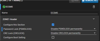
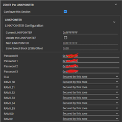
The same for all flash sectors, secured  by zone 1. So the corresponding .asm generated file is:

;----------------------------------------------------------------------
; Zone 1
;----------------------------------------------------------------------
.sect "dcsm_otp_z1_linkpointer"
.retain
.long 0x1FFFFFFF
.long 0xFFFFFFFF ;Reserved
.long 0x1FFFFFFF
.long 0xFFFFFFFF ;Reserved
.long 0x1FFFFFFF
.long 0xFFFFFFFF ;Reserved

.sect "dcsm_otp_z1_pswdlock"
.retain
.long 0xFFFFFFFF
.long 0xFFFFFFFF ;Reserved

.sect "dcsm_otp_z1_crclock"
.retain
.long 0xFFFFFFFF
.long 0xFFFFFFFF ;Reserved

;; .sect "dcsm_otp_z1_bootctrl"
;; .retain
;; .long 0xFFFFFFFF ;Reserved
;; .long 0x49550B5A

.sect "dcsm_zsel_z1"
.retain
.long 0x000000FF ;Z1-EXEONLYRAM
.long 0x00003FFF ;Z1-EXEONLYSECT
.long 0x10005555 ;Z1-GRABRAM
.long 0x05555555 ;Z1-GRABSECT

.long 0x--- (PASSWORDS)
.long 0x-----
.long 0x----
.long 0x----

I checked that doing this, then all these sectors of memory are secured, I can connect through JTAG but I can't read memory. My LINKPOINTER is 0x20. That's ok.

The problem is that now I wanted to lock passwords in order to make them not visible through any access. I wanted to do it by changing :
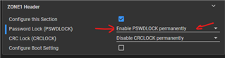
But when I try to load the  program with this change in PSWDLOCK I have this error:

C28xx_CPU1: If erase/program (E/P) operation is being done on one core, the other core should not execute from shared-RAM (SR) as they are used for the E/P code. Also, CPU1 will be halted to determine SR ownership for the CPU which will run the Flash Plugin code, after which CPU1 will be set to run its application. User code execution from SR could commence after both flash banks are programmed.
C28xx_CPU1: Error during Flash programming (Flash algorithm returned error code). FMSTAT (STATCMD on some devices) value = 48. Operation Cancelled (0).
C28xx_CPU1: File Loader: Memory write failed: Unknown error
C28xx_CPU1: GEL: File: C:\Users\mserrataco\Documents\01 SOFTWARE\02_SW_BootloaderCAN_DualCore\cpu1\Debug_CPU1\bootloader_cpu_cpu1.out: Load failed.

In Flash Settings I set the actual LINKPOINTER at 0x20 and the custom passwords:

So these are my questions:

1. As enabling PSWDLOCK changes from 1 to 0 last four bits, I thought it was always programmable. Is that true? 

2. If not, is it possible to make something to this device to secure this password or it is impossible from now?

Thank you

  • 1. As enabling PSWDLOCK changes from 1 to 0 last four bits, I thought it was always programmable. Is that true? 

    If  you are asking whether PSWDLOCK register is re-programmable, the answer is “No”. The OTP is one-time-programmable and hence, can be programmed only once.

    2. If not, is it possible to make something to this device to secure this password or it is impossible from now?

    Going through your post, it appears you  have already secured the device, so I don’t understand your question. 

    These 4 easy-to-understand videos explain how the DCSM module works:  

    https://www.ti.com/video/6336140498112?keyMatch=DCSM

    https://www.ti.com/video/6336138543112?keyMatch=DCSM

    https://www.ti.com/video/6336139910112?keyMatch=DCSM

    https://www.ti.com/video/6336139622112?keyMatch=DCSM

  • Hello Hareesh, 

    thanks for you answer. According to question 2,  secured my device but the passwords are visible if I connect through JTAG (I can connect with "Wait boot mode" status and without introducing password in CSMPSWD of Flash Settings). So, with my secured device:

    • I can connect through JTAG
    • I can read passwords at adress 0x78028 --> this is what I don't want
    • I can't read the rest of memory (all addresses show 0x0000) without introducing correct CSMPSWD in flash settings
    • I can't load new .out without introducing correct CSMPSWD in flash settings

    So my question was related to second item, I didn't want to be able to read passwords through JTAG without introducing the correct CSMPSWD.I thought I would be able to change PSWDLOCK at the end of my debug process in order to block this passwords, but I don't know if it is already possible or not.

    Thank you

  • Etiam,

                I believe I understand the issue. I have a feeling you are stuck with the same issue as https://e2e.ti.com/support/microcontrollers/c2000-microcontrollers-group/c2000/f/c2000-microcontrollers-forum/1271793/tms320f28379d-problem-with-programming-otp_pswdlock.

    • I can connect through JTAG
    • I can read passwords at adress 0x78028 --> this is what I don't want

    Understandable, since you have programmed the passwords but not enabled security yet, which is done by writing to the PSWDLOCK register.

    I can't read the rest of memory (all addresses show 0x0000) without introducing correct CSMPSWD in flash settings

    Expected since the secure resources are not unsecured until the Password Match Flow (PMF) is executed

    I can't load new .out without introducing correct CSMPSWD in flash settings

    This is expected as well. You cannot program the Flash until you have unsecured it.

    Did you program the whole OTP in one attempt or did you try to program the security settings first and the PSWDLOCK later?

  • Hareesh,

    the first time I programmed the device was with this dcsm.asm file , so I think I programmed all the security settings including PSWDLOCK (even it was 0xFFFFFFFF).

    ;----------------------------------------------------------------------
    ; Zone 1
    ;----------------------------------------------------------------------
         .sect "dcsm_otp_z1_linkpointer"
          .retain
          .long 0x1FFFFFFF
          .long 0xFFFFFFFF     ;Reserved
          .long 0x1FFFFFFF
          .long 0xFFFFFFFF     ;Reserved
          .long 0x1FFFFFFF
          .long 0xFFFFFFFF     ;Reserved
        
         .sect "dcsm_otp_z1_pswdlock"
          .retain
          .long 0xFFFFFFFF
          .long 0xFFFFFFFF     ;Reserved
          
         .sect "dcsm_otp_z1_crclock"
          .retain
          .long 0xFFFFFFFF
          .long 0xFFFFFFFF     ;Reserved
       
    ;;     .sect "dcsm_otp_z1_bootctrl"
    ;;      .retain
    ;;      .long 0xFFFFFFFF     ;Reserved
    ;;      .long 0x49550B5A
          
         .sect "dcsm_zsel_z1"
          .retain
          .long 0x000000FF       ;Z1-EXEONLYRAM
          .long 0x00003FFF      ;Z1-EXEONLYSECT
          .long 0x10005555          ;Z1-GRABRAM
          .long 0x05555555         ;Z1-GRABSECT
          
          .long 0x--------  ; my custom passwords
          .long 0x--------
          .long 0x--------
          .long 0x--------
    

    My dcsm.cmd file was:

    MEMORY
    {
    PAGE 0 :  /* Program Memory */
    
       /* Z1 OTP.  LinkPointers */
       DCSM_OTP_Z1_LINKPOINTER   : origin = 0x78000, length = 0x00000C
       /* Z1 OTP.  GPREG1/GPREG2 */
       DCSM_OTP_Z1_GPREG         : origin = 0x7800C, length = 0x000004
       /* Z1 OTP.  PSWDLOCK/RESERVED */
       DCSM_OTP_Z1_PSWDLOCK	    : origin = 0x78010, length = 0x000004
       /* Z1 OTP.  CRCLOCK/RESERVED */
       DCSM_OTP_Z1_CRCLOCK	    : origin = 0x78014, length = 0x000004
       /* Z1 OTP.  RESERVED/BOOTCTRL */
       DCSM_OTP_Z1_BOOTCTRL	    : origin = 0x7801C, length = 0x000004
    
       /* DCSM Z1 Zone Select Contents (!!Movable!!) */
       /* Z1 OTP.  Z1 password locations / Flash and RAM partitioning */
       DCSM_ZSEL_Z1_P0	        : origin = 0x78020, length = 0x000010
    
       /* Z2 OTP.  LinkPointers */
       DCSM_OTP_Z2_LINKPOINTER	: origin = 0x78200, length = 0x00000C
       /* Z2 OTP.  GPREG1/GPREG2 */
       DCSM_OTP_Z2_GPREG	        : origin = 0x7820C, length = 0x000004
       /* Z2 OTP.  PSWDLOCK/RESERVED */
       DCSM_OTP_Z2_PSWDLOCK	    : origin = 0x78210, length = 0x000004
       /* Z2 OTP.  CRCLOCK/RESERVED */
       DCSM_OTP_Z2_CRCLOCK	    : origin = 0x78214, length = 0x000004
       /* Z2 OTP.  GPREG3/BOOTCTRL */
       DCSM_OTP_Z2_BOOTCTRL	    : origin = 0x7821C, length = 0x000004
    
       /* DCSM Z2 Zone Select Contents (!!Movable!!) */
       /* Z2 OTP.  Z2 password locations / Flash and RAM partitioning  */
       DCSM_ZSEL_Z2_P0	        : origin = 0x78220, length = 0x000010
    
    }
    
    SECTIONS
    {
       dcsm_otp_z1_linkpointer 	: > DCSM_OTP_Z1_LINKPOINTER		PAGE = 0
       dcsm_otp_z1_pswdlock		: > DCSM_OTP_Z1_PSWDLOCK		PAGE = 0
       dcsm_otp_z1_crclock		: > DCSM_OTP_Z1_CRCLOCK			PAGE = 0
       dcsm_otp_z1_bootctrl		: > DCSM_OTP_Z1_BOOTCTRL		PAGE = 0, type = DSECT
       dcsm_zsel_z1				: > DCSM_ZSEL_Z1_P0				PAGE = 0
    
       dcsm_otp_z2_linkpointer	: > DCSM_OTP_Z2_LINKPOINTER		PAGE = 0, type = DSECT
       dcsm_otp_z2_pswdlock		: > DCSM_OTP_Z2_PSWDLOCK		PAGE = 0, type = DSECT
       dcsm_otp_z2_crclock		: > DCSM_OTP_Z2_CRCLOCK			PAGE = 0, type = DSECT
       dcsm_otp_z2_bootctrl		: > DCSM_OTP_Z2_BOOTCTRL		PAGE = 0, type = DSECT
       dcsm_zsel_z2				: > DCSM_ZSEL_Z2_P0				PAGE = 0, type = DSECT
    }
    

    I will read the post you mentioned, thank you.

    Another last question, do I have to do this in dcsm.asm file prior to production?

    ; For code security operation,after development has completed, prior to
    ; production, all other zone select block locations should be programmed
    ; to 0x0000 for maximum security.
    ; If the first zone select block at offset 0x10 is used, the section
    ; "dcsm_rsvd_z1" can be used to program these locations to 0x0000.
    ; This code is commented out for development.
    
    ; .sect "dcsm_rsvd_z1"
    ; .loop (1e0h)
    ; .int 0x0000
    ; .endloop


    I don't understand two things about this code:

    1. Why the first zone select block is 0x10, I thought the first one was 0x20. 

    2. If i'm using another zone select block, do I have to change de value of  .loop(1e0h), right?

    Thank you very much

  • Etiam,

       Please give me a day or two to analyze this.

  • Hi Etiam,

    Have you tried all of the following before attempting to program the .out file that has PSWDLOCK enabled?

    • Unlock the zone via the On-Chip flash tool before programming new .out file that has PSWDLOCK enabled.
    • Power-cycle the device before programming .out file
    • Make sure both CPUs have been reset and are not running before programming new .out file

    Thank you,

    Luke

  • Etiam,

         You need to exclude programming the PSWDLOCK when you programmed the other zone settings. Even though you did not change the value of the PSWDLOCK register, the tool updates the corresponding ECC, which then would prevent you from writing to the PSWDLOCK again. You have two choices:

    1. Exclude PSWDLOCK initially.
    2. Write everything (zone settings and zone header) in one go.