


Hello TI Support Team,
I have take a look to the following TI documents
- C2000
 F28P65x Series LaunchPad Development Kit
 - TMS320F28P65x Real-Time Microcontrollers , Technical Reference Manual
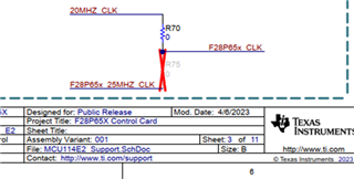
- F28P65X Control Card
and I would like to ask your support about some points.
Based on my understanding ESC EtherCat runs inside F28P65: please can you confirm ?
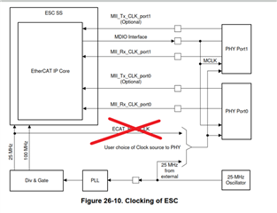
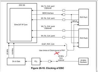
Further, I find four options for EtherCat electrical diagram: please refer to the next options.
Option 1
One oscillator provides clock to ESC and PHYs devices, as shown on the next pictures.

Option 2
One oscillator provides clock to ESC.
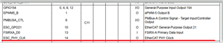
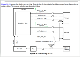
ESC provides clock to PHY devices through GPIO154, as shown on the next pictures.
Option 3
One oscillator for the EtherCat PHYs
One oscillator for the Dsp
Ethercat PHYs

CPU oscillator

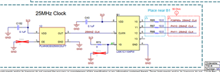
Option 4
Based on my understanding, user manual doesn’t describe this configuration: please look at on the "Questions part".
Questions
Assuming that my logic board works on electromagnetic harsh environment, can you suggest the best Ethercat electrical diagram ?
Regarding the PCB layout, assuming that we do not want sharing high frequency clock signal through a long net, can you also suggest the best electrical diagram ?
F28P65 peripheral manual, doesn’t state about the clock generation or distribution shown by the electrical diagram on option 3: am I correct ? If yes, why ?
Given the configuration shown on “Option 4” , please can you describe:
- the features of MII_Tx_CLK_port1 and MII_Tx_CLK_port0
- how these two optional connections affects the clock generation ? I mean is the clock over the red net still necessary ?
Thank you very much for your support,
Ettore

