Hi Champ,
I am asking for my customer.
The source of 3.3V is supplied by DC source to JTAG 14 pin header.
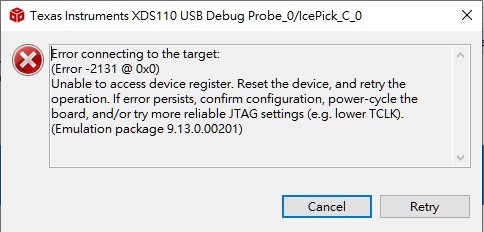
The test connection in target configuration is shown "The JTAG IR Integrity scan-test has succeeded." , while to program a new device on customer's own board, there is an error shown as below. The JTAG schematic is also shown below, C80 & R59 are removed.

Look into customer's schematic, it was found out the boot pins (GPIO24&32) weren't initially pull high to 1 as flash boot.
(1). I am asking if the boot pins weren't set properly to boot to flash, could the image be programmed successfully via XDS110 into a new device ? Or the two things are independent and not relative to each other ?
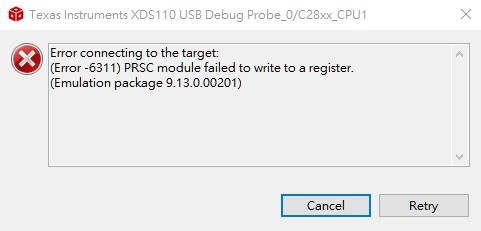
(2). After asking customer to both PU to 3.3V on GPIO24&32, the new device wasn't still unavailable to program with below new error. From other C2k series DS, such as F2837x, there is a note for The default behavior of Get mode is boot-to-flash. On unprogrammed devices, using Get mode will result in repeated watchdog resets, which may prevent proper JTAG connection and device initialization. Use Wait mode or another boot mode for unprogrammed devices. Is it still valid for F280013x if we try to program a new unprogrammed device ?

(3). What is the troubleshoot or place to dive into to address such unable to program a new device ?
Thanks and regards,
Johnny

