This thread has been locked.

If you have a related question, please click the "Ask a related question" button in the top right corner. The newly created question will be automatically linked to this question.

TMS320F2800137: PPM

Part Number: TMS320F2800137

Hi expert,

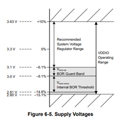
A. In the figure6-5, what does 2.80V stand for?

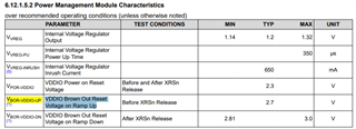
B. In the table6.12.1.5.2, VBOR-VDDIO-UP is 2.7V, does it mean chip release BOR at 2.7V while power on?

C. In the table6.12.1.5.2, VBOR-VDDIO-DN is 2.81~3.0V, does it mean chip trigger BOR around 2.81~3.0V while power down?

D. In the figure6-5, what does BOR Guard Band stand for? After the chip release BOR at 3.0V, the chip is still not at the recommended voltage?

  • Hi Anka,

    Please allow me to get back to you about this next Monday when I am back in office. I apologize for the delay.

    Best Regards,

    Ben Collier

  • Anka,

    A. The illustration is trying to show that the BOR circuit will reset the device before VDDIO leaves the operating range for the device. In this diagram, 2.80V represents the minimum VDDIO operating voltage. A voltage between 3.0V and 2.8V will trigger a BOR so that the device is reset before leaving the VDDIO safe operating range. The exact voltage for a BOR will vary chip to chip. 

    B.  At 2.7V, the internal voltage regulator is enabled and the core is powered. There are checks to see if VDD is at the expected voltage before the chip is released from reset.

    C. That is correct, the device will reset in this range.

    D. The BOR guard band is the voltage difference between the minimum recommended voltage regulator output for VDDIO and the maximum voltage at which the BOR reset may be triggered. The chip can operate in this region, but it is not recommended since small glitches may trigger a BOR reset.

    Best Regards,

    Ben Collier