


TMS320F280025C
Basic information: A total of 8 PWM outputs, of which 4 PWM outputs PWM1A, PWM2B, PWM3B, and PWM4A output the same waveform; 4 PWM1B, PWM2A, PWM3A, and PWM4B output the same waveform;
the first 4 channels and the last 4 channels are complementary outputs and have dead zones. Time 1 microsecond.
Problems: Now it is necessary to make the rising edge of PWM1A and PWM2B 500 nanoseconds earlier than PWM3B and PWM4A, and the falling edge 500 nanoseconds later than PWM3B and PWM4A. The waveform is as shown in the figure; at the same time, it is also necessary to make the rising edge of PWM1B and PWM2A earlier 500 nanoseconds than PWM3A and PWM4B, the falling edge is 500 nanoseconds later than PWM3A and PWM4B, and the waveform is the same as Figure 1.
Difficulty: PWM1A, PWM1B, PWM2A and PWM2B are complementary waveforms, and now their duty cycles are all required to be larger than the other two waveforms.
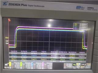
Note: The blue and purple waveforms are PWM1A and PWM2B, and the green waveforms are PWM3B and PWM4A.
Whether there is a solution?

