


Part Number: LAUNCHXL-F28379D
I have wanting to get SPI_DMA working on the LaunchXL-F28379D. I have looked at the example for spi_dma loopback and DMA_SGRAM example. I am working with transmitting 8 bits over SPI at a time for the device I am using. I have ran into a few problems with how DMA is working. I can get 1-17 words to send over the 8 bit SPI via DMA just fine. It is just when I want to send more data it starts dropping values. I am wanting to send 32 bytes of data. I am using generic values of 1-32 to see if I get all the values. 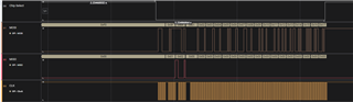
The picture above shows that when I send 17 values they are all sent correctly. The 0cF0, 0x5F, and 0xE8 are not sent via DMA. The DMA starts at 0x01 and ends at 0x17.
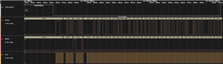
The above picture shows that when I send 32 words from 1-32 they are cut off. This happens for every value of 17. The first 3 bytes of data are not DMA. The DMA transfer starts at 0x01 and ends with 0x32.
Below is my code for SPI initialization and the DM.
SPI:
GPIO_SetupPinMux(66, GPIO_MUX_CPU1, 0); // SPIB CS
GPIO_SetupPinOptions(66, GPIO_OUTPUT, GPIO_PUSHPULL); // SPIB CS
GpioDataRegs.GPCSET.bit.GPIO66 = 1; //SPIB CS
GPIO_setPinConfig(GPIO_63_SPISIMOB);
GPIO_setPinConfig(GPIO_64_SPISOMIB);
GPIO_setPinConfig(GPIO_65_SPICLKB);
// GPIO_setPinConfig(GPIO_66_SPISTEB); // Configured above to set low when needed
// ASYNC Mode
GPIO_setQualificationMode(63, GPIO_QUAL_ASYNC);
GPIO_setQualificationMode(64, GPIO_QUAL_ASYNC);
GPIO_setQualificationMode(65, GPIO_QUAL_ASYNC);
// GPIO_setQualificationMode(66, GPIO_QUAL_ASYNC); // Configured above
SPI_disableModule(SPIB_BASE);
// SPI_enableHighSpeedMode(SPIB_BASE);
SPI_setConfig(SPIB_BASE, DEVICE_LSPCLK_FREQ, SPI_PROT_POL1PHA0,
SPI_MODE_MASTER, 1250000, 8); //1250000
// SpibRegs.SPIFFTX.bit.TXFFIL = 8;
// SpibRegs.SPIFFRX.bit.RXFFIL = 8; // Set RX FIFO level
//
// SpibRegs.SPIFFTX.bit.SPIFFENA = 1;
// SpibRegs.SPIFFTX.bit.TXFFINTCLR = 1;
// SpibRegs.SPIFFRX.bit.RXFFINTCLR = 1;
// SpibRegs.SPIFFRX.bit.RXFFOVFCLR = 1;
// SpibRegs.SPIFFTX.bit.TXFIFO = 1;
// SpibRegs.SPIFFRX.bit.RXFIFORESET = 1;
// SpibRegs.SPIFFTX.bit.SPIRST = 1;
//// SPI_enableFIFO(SPIB_BASE);
SpibRegs.SPIFFRX.all=0x2040; // RX FIFO enabled, clear FIFO int
SpibRegs.SPIFFRX.bit.RXFFIL = 8; // Set RX FIFO level
SpibRegs.SPIFFTX.all=0xE040; // FIFOs enabled, TX FIFO released,
SpibRegs.SPIFFTX.bit.TXFFIL = 8; // Set TX FIFO level
SPI_clearInterruptStatus(SPIB_BASE, SPI_INT_RXFF);
// SPI_setFIFOInterruptLevel(SPIB_BASE, SPI_FIFO_TXEMPTY, SPI_FIFO_RX3);
SPI_setFIFOInterruptLevel(SPIB_BASE, SPI_FIFO_TXEMPTY, SPI_FIFO_RX2);
//SPI_enableLoopback(SPIB_BASE);
SPI_disableLoopback(SPIB_BASE);
SPI_setEmulationMode(SPIB_BASE, SPI_EMULATION_FREE_RUN);
SPI_enableModule(SPIB_BASE);
// // Release the SPI from reset
// SpibRegs.SPICCR.bit.SPISWRESET = 1;
// Falling edge interrupt
GPIO_setInterruptType(GPIO_INT_XINT2, GPIO_INT_TYPE_RISING_EDGE);
GPIO_enableInterrupt(GPIO_INT_XINT2); // Enable XINT2
EALLOW;
CpuSysRegs.PCLKCR0.bit.DMA = 1; /* DMA */
CpuSysRegs.SECMSEL.bit.PF2SEL = 1;
/* Initialize DMA */
DmaRegs.DMACTRL.bit.HARDRESET = 1; /* Perform a hard reset on the DMA */
asm(" NOP"); /* one NOP is required after a hard reset */
DmaRegs.DEBUGCTRL.bit.FREE = 1; /* Allow DMA to run free on emulation suspend */
EDIS;
DMA_initController();
//
// Enable Global Interrupt (INTM) and realtime interrupt (DBGM)
//
EINT;
ERTM;
EALLOW;
// /* Initialize DMA */
// DmaRegs.DMACTRL.bit.HARDRESET = 1; /* Perform a hard reset on the DMA */
// asm(" NOP"); /* one NOP is required after a hard reset */
// DmaRegs.DEBUGCTRL.bit.FREE = 0; /* Allow DMA to run free on emulation suspend */
/* Setup the Source Address */
DmaRegs.CH5.SRC_BEG_ADDR_SHADOW = (uint32_t)Data;
DmaRegs.CH5.SRC_ADDR_SHADOW = (uint32_t)Data;
/* Setup the Destination Address */
DmaRegs.CH5.DST_BEG_ADDR_SHADOW = (uint32_t)(&(SpibRegs.SPITXBUF));
DmaRegs.CH5.DST_ADDR_SHADOW = (uint32_t)(&(SpibRegs.SPITXBUF));
/* Configure Burst Mode for a single 16 bit value*/
DmaRegs.CH5.BURST_SIZE.bit.BURSTSIZE = 7; // Actual Size is BURSTSIZE + 1
DmaRegs.CH5.SRC_BURST_STEP = 1; // Add one to the source address after a burst
DmaRegs.CH5.DST_BURST_STEP = 0; // Do not increment the destination address after a burst
/* Configure Transfer */
// DmaRegs.CH1.TRANSFER_SIZE = EXC_STEPS_PER_PERIOD; // How many bursts per transfer
DmaRegs.CH5.TRANSFER_SIZE =3;
DmaRegs.CH5.SRC_TRANSFER_STEP = 1; // Add one to the source address after a transfer
DmaRegs.CH5.DST_TRANSFER_STEP = 0; // Do not change the address of the destination after a transfer
/* Configure Source Wrapping */
DmaRegs.CH5.SRC_WRAP_SIZE = 0xFFFF; // Wrap back to beginning after 32 transfers
DmaRegs.CH5.SRC_WRAP_STEP = 0; // Go back to the first index
DmaRegs.CH5.DST_WRAP_SIZE = 0xFFFF;
DmaRegs.CH5.DST_WRAP_STEP = 0; // Go back to the first index
/* Configure the DMA Mode */
DmaClaSrcSelRegs.DMACHSRCSEL2.bit.CH5 = 0; // Configure DMA Ch 1 to trigger off software
DmaRegs.CH5.MODE.bit.PERINTSEL = 5; // DMA Channel
DmaRegs.CH5.MODE.bit.PERINTE = 1; // Enable peripheral event trigger
DmaRegs.CH5.MODE.bit.ONESHOT = 1; // Performs an entire transfer instead of just one burst per trigger
DmaRegs.CH5.MODE.bit.CONTINUOUS = 1; // If set to one DMA reinitializes once TRANSFER_COUNT is zero
DmaRegs.CH5.MODE.bit.OVRINTE = 0; // Disable interrupt on overflow event
DmaRegs.CH5.MODE.bit.DATASIZE = 0; // 0 = 16-bit data size, 1 = 32-bit data size
DmaRegs.CH5.MODE.bit.CHINTMODE = 1; // 0 = Interrupt at beginning, 1 = Interrupt and end of transfer
DmaRegs.CH5.MODE.bit.CHINTE = 1; // Enable/Disable interrupt
DmaRegs.CH5.CONTROL.bit.PERINTCLR = 1; // Clear any interrupt flags
DmaRegs.CH5.CONTROL.bit.ERRCLR = 1; // Clear any error flags
/* Setup the Source Address */
DmaRegs.CH6.SRC_BEG_ADDR_SHADOW = (uint32_t)(&(SpibRegs.SPIRXBUF));
DmaRegs.CH6.SRC_ADDR_SHADOW = (uint32_t)(&(SpibRegs.SPIRXBUF));
/* Setup the Destination Address */
DmaRegs.CH6.DST_BEG_ADDR_SHADOW = (uint32_t)DMA_test;
DmaRegs.CH6.DST_ADDR_SHADOW = (uint32_t)DMA_test;
/* Configure Burst Mode for a single 16 bit value*/
DmaRegs.CH6.BURST_SIZE.bit.BURSTSIZE = 7; // Actual Size is BURSTSIZE + 1
DmaRegs.CH6.SRC_BURST_STEP = 0; // Add one to the source address after a burst
DmaRegs.CH6.DST_BURST_STEP = 0; // Do not increment the destination address after a burst
/* Configure Transfer */
// DmaRegs.CH1.TRANSFER_SIZE = EXC_STEPS_PER_PERIOD; // How many bursts per transfer
DmaRegs.CH6.TRANSFER_SIZE = 3;
DmaRegs.CH6.SRC_TRANSFER_STEP = 0; // Add one to the source address after a transfer
DmaRegs.CH6.DST_TRANSFER_STEP = 0; // Do not change the address of the destination after a transfer
/* Configure Source Wrapping */
DmaRegs.CH6.SRC_WRAP_SIZE = 0xFFFF; // Wrap back to beginning after 32 transfers
DmaRegs.CH6.SRC_WRAP_STEP = 0; // Go back to the first index
DmaRegs.CH6.DST_WRAP_SIZE = 0xFFFF;
DmaRegs.CH6.DST_WRAP_STEP = 0; // Go back to the first index
/* Configure the DMA Mode */
DmaClaSrcSelRegs.DMACHSRCSEL2.bit.CH6 = DMA_TRIGGER_SPIBRX; // Configure DMA Ch 6 to trigger off SPIRX
DmaRegs.CH6.MODE.bit.PERINTSEL = 6; // DMA Channel
DmaRegs.CH6.MODE.bit.PERINTE = 1; // Enable peripheral event trigger
DmaRegs.CH6.MODE.bit.ONESHOT = 1; // Performs an entire transfer instead of just one burst per trigger
DmaRegs.CH6.MODE.bit.CONTINUOUS = 1; // If set to one DMA reinitializes once TRANSFER_COUNT is zero
DmaRegs.CH6.MODE.bit.OVRINTE = 0; // Disable interrupt on overflow event
DmaRegs.CH6.MODE.bit.DATASIZE = 0; // 0 = 16-bit data size, 1 = 32-bit data size
DmaRegs.CH6.MODE.bit.CHINTMODE = 1; // 0 = Interrupt at beginning, 1 = Interrupt and end of transfer
DmaRegs.CH6.MODE.bit.CHINTE = 0; // Enable/Disable interrupt
DmaRegs.CH6.CONTROL.bit.PERINTCLR = 1; // Clear any interrupt flags
DmaRegs.CH6.CONTROL.bit.ERRCLR = 1; // Clear any error flags
EDIS;
EALLOW;
/* Start DMA on Channel 1 */
DmaRegs.CH5.CONTROL.bit.RUN = 1;
asm(" NOP");
DmaRegs.CH6.CONTROL.bit.RUN = 1;
asm(" NOP");
DmaRegs.CH5.CONTROL.bit.PERINTFRC = 1;
asm(" NOP");
EDIS;
Thank you in advance for your help!


