Part Number: TMS320F28335
I am using the Mcbsp as an SPI master in clock stop mode. I set up the peripheral as described by the Example_2833xMcBSP_SPI_DLB.c just not in loopback and 8 bit data. For some reason the code i inherited is set up to use the gpio as a chip select but it is only connected to a single device so I can set it active low the whole time.
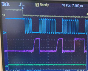
The problem is that I see clock signals at the beginning and end of my sequence that are less than 8. I included scope plots for review. Thanks
// McBSP-A register settings
McbspaRegs.SPCR2.all=0x0000; // Reset FS generator, sample rate generator & transmitter
McbspaRegs.SPCR1.all=0x0000; // Reset Receiver, Right justify word, Digital loopback dis.
McbspaRegs.PCR.all=0x0F08; //(CLKXM=CLKRM=FSXM=FSRM= 1, FSXP = 1)
//McbspaRegs.SPCR1.bit.DLB = 1;
McbspaRegs.SPCR1.bit.CLKSTP = 2; // Together with CLKXP/CLKRP determines clocking scheme
McbspaRegs.PCR.bit.CLKXP = 0; // CPOL = 0, CPHA = 0 rising edge no delay
McbspaRegs.PCR.bit.CLKRP = 0;
McbspaRegs.RCR2.bit.RDATDLY=01; // FSX setup time 1 in master mode. 0 for slave mode (Receive)
McbspaRegs.XCR2.bit.XDATDLY=01; // FSX setup time 1 in master mode. 0 for slave mode (Transmit)
McbspaRegs.RCR1.bit.RWDLEN1=0; // 8-bit word
McbspaRegs.XCR1.bit.XWDLEN1=0; // 8-bit word
McbspaRegs.SRGR2.all=0x2000; // CLKSM=1, FPER = 1 CLKG periods
//McbspaRegs.SRGR1.all= 0x000F; // Frame Width = 1 CLKG period, CLKGDV=16, 100MHz/16 = 6.25MHz
//McbspaRegs.SRGR1.all= 0x000A; // Frame Width = 1 CLKG period, CLKGDV=8, 100MHz/8 = 12.5MHz
McbspaRegs.SRGR1.all= 0x00040; // Frame Width = 1 CLKG period, CLKGDV=64, 100MHz/64 = 1.5MHz 6.5us
//McbspaRegs.RCR2.bit.RFIG = 1; // Ignore frame sync signals
//McbspaRegs.XCR2.bit.XFIG = 1; // Ignore frame sync signals
McbspaRegs.SPCR2.bit.GRST=1; // Enable the sample rate generator
delay_loop(); // Wait at least 2 SRG clock cycles
McbspaRegs.SPCR2.bit.XRST=1; // Release TX from Reset
McbspaRegs.SPCR1.bit.RRST=1; // Release RX from Reset
McbspaRegs.SPCR2.bit.FRST=1; // Frame Sync Generator reset