Other Parts Discussed in Thread: ADS8686S, ADS8686SEVM-PDK, , SYSCONFIG, C2000WARE
Good morning, colleagues,
I am new to programming on Texas microcontrollers. I am programming a TMS320F28388D with its Docking Card. I want to communicate via SPI with a TI ADC, specifically the ADS8686S with its ADS8686SEVM-PDK evaluation board.
This ADC allows SPI communication via two channels SDOA for ADCA and SDOB for ADCB but I want to use only 1, so reading the datasheet, I ground SDOB and in SDOA the two conversions are sent.
My problem has to do with the SPI communication itself. I have made a code with which I basically want to perform some very basic functionalities:
1. First, write in the ADC registers to configure it the way I want (configuration, input voltage range, type of low pass filter, etc...).
2. Send it to convert a channel and have it give me back the conversion.
This ADC makes use of the SPI communication signals (PICO, POCI, SCLK, CS(GPIO output)), CONVST (GPIO output), BUSY (GPIO input) and they are used according to what is shown in the ADC datasheet timing diagram. I have made a code with the help of sysconfig (I am still very inexperienced) and it compiles the code. However, when I connect the two devices and connect the signals I see that it gets stuck in this loop.
I have checked with the oscilloscope that the SCLK output of the microcontroller is at 0, it does not generate clock pulses. I would like to know if you could help me with this code. Basically, reading the ADC datasheet I think it works as follows:
1. Write to ADC register:
- Set to 1 convst for a small period of 50ns.
- Subsequently, enable SPI communication by setting CS to 0. CLEAR
- The SPI frame is sent with the register to be configured.
- Wait to receive an interrupt FLAG for reception.
- Go to the interrupt routine to receive the message from the ADC and clear the flags.
- The CS is deactivated by setting 1.
2. Read ADC conversion:
- Set to 1 convst for a small period of 50ns.
- When set to 1 convst the ADC returns the Busy signal to 1 until the conversion is finished.
- When Busy returns to 0, i.e. when the conversion is finished, SPI communication is enabled by setting CS to 0. CLEAR
- Wait to receive a receive interrupt FLAG.
- Go to the interrupt routine to receive the ADC conversion and clear the flags.
- The CS is deactivated by setting it to 1. SET
I leave you the code I have done and the sysconfig, in case you can see why the clock signal is not even sent with the ADC, although in the debug it gets stuck in the while part of the interrupt flag.
#include "driverlib.h"
#include "device.h"
#include "board.h"
#include "f2838x_device.h"
//#include "C:/ti/c2000/C2000Ware_5_00_00_00/device_support/f2838x/headers/include/f2838x_device.h"
//#include "F28x_Project.h"

//#include "F2838x_PieCtrl.h"
//
//
//

#ifdef __cplusplus
#pragma DATA_SECTION("SpiaRegsFile")
#else
#pragma DATA_SECTION(SpiaRegs,"SpiaRegsFile");
#endif
volatile struct SPI_REGS SpiaRegs;

#ifdef __cplusplus
#pragma DATA_SECTION("GpioDataRegsFile")
#else
#pragma DATA_SECTION(GpioDataRegs,"GpioDataRegsFile");
#endif
volatile struct GPIO_DATA_REGS GpioDataRegs;


#ifdef __cplusplus
#pragma DATA_SECTION("PieVectTableFile")
#else
#pragma DATA_SECTION(PieVectTable,"PieVectTableFile");
#endif
volatile struct PIE_VECT_TABLE PieVectTable;

#ifdef __cplusplus
#pragma DATA_SECTION("DacaRegsFile")
#else
#pragma DATA_SECTION(DacaRegs,"DacaRegsFile");
#endif
volatile struct DAC_REGS DacaRegs;


volatile Uint16 lecturadatoADCdummy;
volatile Uint16 flag_conf_noconversion=1;
volatile Uint16 lecturaconvADCA;
volatile Uint16 lecturaconvADCB;

volatile Uint16 comandoADCconf;

Uint16 tramaConfADC=((1 << 15) | (0x2 << 9) | (0x0));     //MANDA TRAMA DE CONFIGURACIÓN DONDE SE DEJA A 0 MODO BURST, SEQEN, OSR, STATUSEN, CRCEN

Uint16 tramaRango_ADCA_0_3=((1 << 15) | (0x4 << 9) | (0x0)); //PONE EL RANGO DE ADC A DEL CANAL 0 AL 3 EN RANGO +-10V
Uint16 tramaRango_ADCA_4_7=((1 << 15) | (0x5 << 9) | (0x0)); //PONE EL RANGO DE ADC A DEL CANAL 4 AL 7 EN RANGO +-10V
Uint16 tramaRango_ADCB_0_3=((1 << 15) | (0x6 << 9) | (0x0)); //PONE EL RANGO DE ADC B DEL CANAL 0 AL 3 EN RANGO +-10V
Uint16 tramaRango_ADCB_4_7=((1 << 15) | (0x7 << 9) | (0x0)); //PONE EL RANGO DE ADC B DEL CANAL 4 AL 7 EN RANGO +-10V

Uint16 tramaFiltroPasoBajo=((1 << 15) | (0xD << 9) | (0x1)); //ESCRIBE FILTRO PASO BAJO DE FRECUENCIA DE CORTE 15kHz | ESCRIBIR 0x0 si se quiere de 39kHz o 0x2 si se quiere de 376kHz

Uint16 conv_ADCA_CH0=((1 << 15) | (0x3 << 9) | (0x0)); //TRAMA QUE ESCRIBE EN REGISTRO PARA ACTIVAR CONVERSIÓN DEL CANAL 0 en ADCA y ADCB. Si se quiere cambiar, ver mapa de registros

Uint16 conv_SEQ_STACK0=((1 << 15) | (0x20 << 9) | (0x0<<8) | (0x0)); //ESCRITURA DE STACK 0 CON SECUENCIA CHA0,CHB0 siguiendo al siguiente Stack
Uint16 conv_SEQ_STACK1=((1 << 15) | (0x21 << 9) | (0x0<<8) | (0x11)); //ESCRITURA DE STACK 1 CON SECUENCIA CHA1,CHB1 siguiendo al siguiente Stack
Uint16 conv_SEQ_STACK2=((1 << 15) | (0x22 << 9) | (0x0<<8) | (0x22)); //ESCRITURA DE STACK 2 CON SECUENCIA CHA2,CHB2 siguiendo al siguiente Stack
Uint16 conv_SEQ_STACK3=((1 << 15) | (0x23 << 9) | (0x0<<8) | (0x33)); //ESCRITURA DE STACK 3 CON SECUENCIA CHA3,CHB3 siguiendo al siguiente Stack
Uint16 conv_SEQ_STACK4=((1 << 15) | (0x24 << 9) | (0x0<<8) | (0x44)); //ESCRITURA DE STACK 4 CON SECUENCIA CHA4,CHB4 siguiendo al siguiente Stack
Uint16 conv_SEQ_STACK5=((1 << 15) | (0x25 << 9) | (0x0<<8) | (0x55)); //ESCRITURA DE STACK 5 CON SECUENCIA CHA5,CHB5 siguiendo al siguiente Stack
Uint16 conv_SEQ_STACK6=((1 << 15) | (0x26 << 9) | (0x0<<8) | (0x66)); //ESCRITURA DE STACK 6 CON SECUENCIA CHA6,CHB6 siguiendo al siguiente Stack
Uint16 conv_SEQ_STACK7=((1 << 15) | (0x26 << 9) | (0x1<<8) | (0x77)); //ESCRITURA DE STACK 7 CON SECUENCIA CHA7,CHB7 Volviendo al Stack 0 si burst mode. Si no, termina secuencia.


// SPI_receive16Bits(uint32_t base, SPI_endianess endianness, uint16_t dummyData, uint16_t txDelay);

// Main
//
volatile Uint16 DatoSPI;


interrupt void INT_SPIADC_EXT_CHAB_RX_ISR(void);
interrupt void INT_SPIADC_EXT_CHAB_TX_ISR(void);


void configuracionADC(void);
void lecturaconvADC(void);

void main(void)
{
    Uint16 comandoADC;


    //
    // Initialize device clock and peripherals
    //
    Device_init();

    //
    // Disable pin locks and enable internal pull ups.
    //
    Device_initGPIO();

    //
    // Initialize PIE and clear PIE registers. Disables CPU interrupts.
    //
    Interrupt_initModule();

    //
    // Initialize the PIE vector table with pointers to the shell Interrupt
    // Service Routines (ISR).
    //
    Interrupt_initVectorTable();


    //
    // Disable sync(Freeze clock to PWM as well)
    //
    SysCtl_disablePeripheral(SYSCTL_PERIPH_CLK_TBCLKSYNC);

    //
    // Configure GPIO0/1 , GPIO2/3 and GPIO4/5 as ePWM1A/1B, ePWM2A/2B and
    // ePWM3A/3B pins respectively
    // Configure EPWM Modules
    //


    Board_init();
    SPI_enableHighSpeedMode(SPIADC_EXT_CHAB_BASE);


    // Enable sync and clock to PWM
    //
    SysCtl_enablePeripheral(SYSCTL_PERIPH_CLK_TBCLKSYNC);

    //
    // Enable ePWM interrupts
    //


    //
    // Enable Global Interrupt (INTM) and realtime interrupt (DBGM)
    //
    EINT;
    ERTM;

    //
    // IDLE loop. Just sit and loop forever (optional):
    //

    PieVectTable.SPIA_RX_INT = &INT_SPIADC_EXT_CHAB_RX_ISR;
    PieVectTable.SPIA_TX_INT = &INT_SPIADC_EXT_CHAB_TX_ISR;
    /////////////////////////////////////////////REALIZAR CONFIGURACIÓN DEL ADC
    configuracionADC();
    ////////////

    //ESCRIBIR EN REGISTRO QUE SE QUIERE CONVERTIR CANAL 0 (TRAMA conv_ADCA_CH0) Y APLICAR SEÑAL DE CONVST


    lecturaconvADC();


    while(1){}


}

void configuracionADC(void){
   //ENVIAR CONFIGURACIÓN DE CONFIGURATION REGISTER 0x2

    GPIO_writePin(CONVST, 1);
     //Debe estar CONV high mínimo 50ns -VISTO EN OSCILOSCOPIO QUE HAY UN DELAY DE 480ns si se ponen seguidos los writepin de CONVST

  //  while (GPIO_readPin(BUSY)==1){} //Se espera a que se ponga a 0 BUSY

    GpioDataRegs.GPACLEAR.bit.GPIO23=1; //CS a 0 se activa.
    GPIO_writePin(CONVST, 0);
    comandoADCconf=tramaConfADC;
    SpiaRegs.SPITXBUF = comandoADCconf;            // Master transmite la configuración
    while(SpiaRegs.SPISTS.bit.INT_FLAG !=1) {} // Espera hasta que envíe todos los bits de la trama.
                                                //INTERRUPCIÓN DE RECEPCIÓN
    GpioDataRegs.GPASET.bit.GPIO23=1; //CS a 0 se desactiva.

    //ENVIAR CONFIGURACIÓN DE RANGO DE CANALES 0-3 DE ADCA

    GPIO_writePin(CONVST, 1);
    GpioDataRegs.GPACLEAR.bit.GPIO23=1; //CS a 0 se activa.
    GPIO_writePin(CONVST, 0);
    comandoADCconf=tramaRango_ADCA_0_3;
    SpiaRegs.SPITXBUF = comandoADCconf;            // Master transmite la configuración
    while(SpiaRegs.SPISTS.bit.INT_FLAG !=1) {} // Espera hasta que envíe todos los bits de la trama.
                                                        //INTERRUPCIÓN DE RECEPCIÓN
    GpioDataRegs.GPASET.bit.GPIO23=1; //CS a 0 se desactiva.

    //ENVIAR CONFIGURACIÓN DE RANGO DE CANALES 4-7 DE ADCA

        GPIO_writePin(CONVST, 1);
        GpioDataRegs.GPACLEAR.bit.GPIO23=1; //CS a 0 se activa.
        GPIO_writePin(CONVST, 0);
        comandoADCconf=tramaRango_ADCA_4_7;
        SpiaRegs.SPITXBUF = comandoADCconf;            // Master transmite la configuración
        while(SpiaRegs.SPISTS.bit.INT_FLAG !=1) {} // Espera hasta que envíe todos los bits de la trama.
                                                            //INTERRUPCIÓN DE RECEPCIÓN
        GpioDataRegs.GPASET.bit.GPIO23=1; //CS a 0 se desactiva.
    //ENVIAR CONFIGURACIÓN DE RANGO DE CANALES 0-3 DE ADCB

        GPIO_writePin(CONVST, 1);
        GpioDataRegs.GPACLEAR.bit.GPIO23=1; //CS a 0 se activa.
        GPIO_writePin(CONVST, 0);
        comandoADCconf=tramaRango_ADCB_0_3;
        SpiaRegs.SPITXBUF = comandoADCconf;            // Master transmite la configuración
        while(SpiaRegs.SPISTS.bit.INT_FLAG !=1) {} // Espera hasta que envíe todos los bits de la trama.
                                                                //INTERRUPCIÓN DE RECEPCIÓN
        GpioDataRegs.GPASET.bit.GPIO23=1; //CS a 0 se desactiva.

     //ENVIAR CONFIGURACIÓN DE RANGO DE CANALES 4-7 DE ADCA

        GPIO_writePin(CONVST, 1);
        GpioDataRegs.GPACLEAR.bit.GPIO23=1; //CS a 0 se activa.
        GPIO_writePin(CONVST, 0);
        comandoADCconf=tramaRango_ADCB_4_7;
        SpiaRegs.SPITXBUF = comandoADCconf;            // Master transmite la configuración
        while(SpiaRegs.SPISTS.bit.INT_FLAG !=1) {} // Espera hasta que envíe todos los bits de la trama.
                                                                        //INTERRUPCIÓN DE RECEPCIÓN
        GpioDataRegs.GPASET.bit.GPIO23=1; //CS a 0 se desactiva.


    //ENVIAR CONFIGURACIÓN DE FILTRO PASO BAJO DE ENTRADA
        GPIO_writePin(CONVST, 1);
        GpioDataRegs.GPACLEAR.bit.GPIO23=1; //CS a 0 se activa.
        GPIO_writePin(CONVST, 0);
        comandoADCconf=tramaFiltroPasoBajo;
        SpiaRegs.SPITXBUF = comandoADCconf;            // Master transmite la configuración
        while(SpiaRegs.SPISTS.bit.INT_FLAG !=1) {} // Espera hasta que envíe todos los bits de la trama.
                                                                                       //INTERRUPCIÓN DE RECEPCIÓN
        GpioDataRegs.GPASET.bit.GPIO23=1; //CS a 0 se desactiva.


         flag_conf_noconversion=0;


}


void lecturaconvADC(void){
    //ENVIAR CONFIGURACIÓN DE CONFIGURATION REGISTER 0x2

    GPIO_writePin(CONVST, 1); //uso de DEVICE_DELAY_US????
    GPIO_writePin(CONVST, 0);     //Debe estar CONV high mínimo 50ns -VISTO EN OSCILOSCOPIO QUE HAY UN DELAY DE 480ns si se ponen seguidos los writepin de CONVST
    while (GPIO_readPin(BUSY)==1){}

    GpioDataRegs.GPACLEAR.bit.GPIO23=1; //CS a 0 se activa.

    while(SpiaRegs.SPISTS.bit.INT_FLAG !=1) {} // Espera hasta que envíe todos los bits de la trama.
                                                    //INTERRUPCIÓN DE RECEPCIÓN
    GpioDataRegs.GPASET.bit.GPIO23=1; //CS a 0 se desactiva.
}


interrupt void INT_SPIADC_EXT_CHAB_RX_ISR(void){
    if (flag_conf_noconversion==1){
        SpiaRegs.SPIFFRX.bit.RXFFOVFCLR=1;  // Clear Overflow flag
        SpiaRegs.SPIFFTX.bit.TXFFINTCLR=1;  // Clear Interrupt flag
        SpiaRegs.SPIFFRX.bit.RXFFINTCLR=1;  // Clear Interrupt flag
       //  FlWaitADC_Ext=0;
        lecturadatoADCdummy = SpiaRegs.SPIRXBUF;     // Read data y resetea flag INT_FLAG

    }
    else{
        SpiaRegs.SPIFFRX.bit.RXFFOVFCLR=1;  // Clear Overflow flag
        SpiaRegs.SPIFFTX.bit.TXFFINTCLR=1;  // Clear Interrupt flag
        SpiaRegs.SPIFFRX.bit.RXFFINTCLR=1;  // Clear Interrupt flag
               //  FlWaitADC_Ext=0;
        lecturaconvADCA = SpiaRegs.SPIRXBUF;     // Read data y resetea flag INT_FLAG
   //     DAC_setShadowValue(, lecturaconvADCA);
    }


 //   PieCtrlRegs.PIEACK.all |= PIEACK_GROUP6;       // Issue PIE ack
}
interrupt void INT_SPIADC_EXT_CHAB_TX_ISR(void){
    SpiaRegs.SPIFFTX.bit.TXFFINTCLR = 1;  // Clear Interrupt flag
  //  PieCtrlRegs.PIEACK.all |= PIEACK_GROUP6;       // Issue PIE ACK
}
I also have doubts about the High-Speed mode and where I can configure that option in the sysconfig, according to the datasheet of the microcontroller, you can reach speeds of 50MHz but then I don't see that option in the sysconfig. What I do is to select the GPIO pins of PICO, POCI, SCLK of ata speed according to the datasheet of the microcontroller but nowhere the "SPICCR.HS_MODE = 1" is applied. If I choose a bitrate of 12.5MHz the program runs until the while loop while if I set it to 50MHz I get an error in SPI_Init().
So basically I would like to figure out the following things: if someone could help me to have a code that I can run on the board for this relatively simple functionality and why I get these errors and if someone could help me on how to implement the High-Speed mode whether it can be done from sysconfig or from sysconfig I would like to know how to implement the High-Speed mode.
I let you the zip with the sysconfig os the project too. I would be very grateful if you could help me. Sorry for maybe some dumb questions. Thank you in advance.
BR,
Pedro
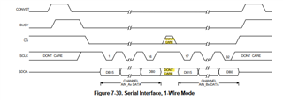
Serial 1-Wire data receive from ADC in SPI
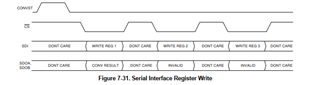
Serial register writting to ADC in SPI