This thread has been locked.

If you have a related question, please click the "Ask a related question" button in the top right corner. The newly created question will be automatically linked to this question.

SiC MOSFET of LLC damaged

Other Parts Discussed in Thread: UCC21520, AMC1301

Hi,Team

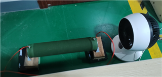
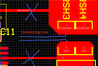
    I designed a LLC prototype with an input of 800V and an output of 200V-750V, with a power of 20kW. The rated output voltage is 650V, and the resonant frequency is 150kHz. The switching frequency ranges from 100kHz to 400kHz, and if it exceeds 400kHz, it is changed to PWM control. At the beginning, 80V input is used, and the output can be adjusted from 20V to 75V, which can achieve hybrid control of PFM and PWM. However, the temperature of the switch tube in the red box in the figure below is relatively high, while the temperature rise of the switch tube in the blue box is almost negligible. Using a fan to blow can control the temperature rise of the red part, and then I conduct a high voltage experiment.
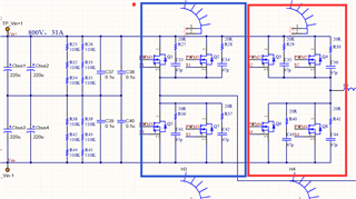
                 Fig.1

When the input voltage rose to 200V, the red part of the SiC MOSFETs was broken. In Figure 1, two SiC MOSFETs with a rated voltage of 1200V and a rated current of 30A were connected in parallel. During the experiment, the power was relatively small, and only one was connected. In Figure 2, the metal pins SiC MOSFETs source pole were all blown out.
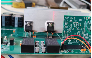
                                    Fig.2

I analyzed the reason and it seems that there is a problem with the buffer circuit. This buffer circuit was used to buffer the switching transistor when I designed PFC before. So I dismantled all the buffer capacitors and redo the experiment with low voltage 80V input. The red part of the SiC MOSFETs in Figure 1 generates heat just like the blue one, without blowing a fan, it didn't generate heat.. Then I raised voltage  to 100V for the experiment, and the output of 80V was OK. When I raised voltage  to 200V , there was no problem with the output of 80V. The second time  the voltage was raised to 200V,SiC MOSFETs damaged again when outputting 160V. This time, the red part in Figure 1 was broken, and a piece of the black part collapsed, as shown in Figure 3
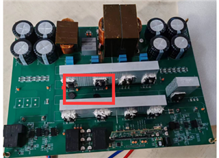
                                  Fig.3

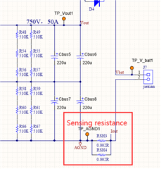
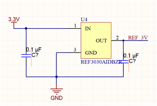
Is it possible that the voltage rise of the 0.1U filtering capacitor in Figure 4 is too fast, or is the voltage rise rate too fast?
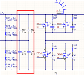
                                Fig.4

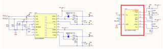
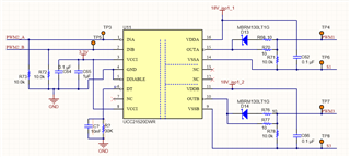
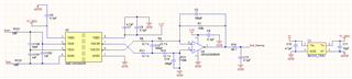
I use UCC21520 as the driver chip for SiC MOS, with a driving voltage of 20V and a dead band of 200ns.
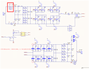
                                 Fig.5

During the experiment, the resistance in the red frame in Figure 5 was not connected and was short circuited. So I'm worried that the voltage rise rate is too fast.

  • the resistance in the red frame in Figure 5 was not connected

    Inrush current only when Ecaps are fully discharged, no issue. Seems more like 440V max, not 880v. Parallel Ecaps has wider plate (doubles µF) but rated working voltage remains 220v for each pair.

    1. Where are resistors for each half bridge to SIC gate lead? 

    2. Are you using AC or DC bus power?

    3. So the XFMR secondary circuit rectified acts as experiment load? 

    4. Why to choose 20v gate drive, what is SIC datasheet Qg graph show and absolute maximum?

  • Hi Fei,

    Our expert is currently Out of Office. We'll get back to you before end of the week. Sorry for the inconvenience. 

    Best,

    Pratik

  • Hi Fei,

    Adding on the questions from Genatco, would you be able to show the surrounding schematic around the gate driver? Seeing the input and output components around the gate driver and knowing what it is driving will help us narrow down where the area of concern is here.

    Looking forward to hearing back!

    Hiroki

  • Hi Genatco,

    Thanks for your reply.

    1. The driving circuit of SiC adopts the driving circuit of TI three-phase Vienna PFC. In the red frame is an isolated power supply that can generate two outputs. The rated voltage of +Vo is 18V, - Vo is -3V. But the actual output voltage of +Vo is 20V, and the FAE of SiC company says 20V is also acceptable. Using -3V during SiC shutdown can shorten the shutdown time, but the driver chip 1ED020I12FA2 that can provide negative voltage is expensive, so I used UCC21520 with a dead time 200ns.

    2. The input voltage is DC.

    3. The output of LLC is connected to high-power cement resistors with different resistance values.

    4. The FAE of SiC company suggested that I use an 18V driving voltage, but 20V is also acceptable, and the resistance of SiC is smaller when the driving voltage is 20V.

  • Hi Adibatla,Honda,

    Thanks for your reply.This video shows the debugging process of inputting 80V and outputting 20V to 75V. Vout divided by 3.93 is the actual voltage value.At the beginning, the reference voltage Vref is 78, representing 20V. I changed the Vref to 157 (40V) and 295 (75V) using CAN simulation software.

    1. Input and output currents cannot be measured. Is the schematic correct? If the red line in the PCB is changed to blue line, can the current be measured?


    2. Online debugging programs and CAN communication are prone to interference, which can lead to interruptions in online debugging and CAN communication, and even cause the computer screen to turn black. Can GND be used to surround the CAN connections?


  • Hi Fei,

    You mentioned a deadtime configuration of 200ns with the UCC21520, and it looks like the resistor selection is correct. However, on the schematic it looks like the deadtime resistor is tied to VCCI instead of ground.

    For deadtime configuration to be properly activated, the resistor must be connected to ground. It is also recommended to add a capacitor in parallel to the deadtime resistor for noise immunity. A ceramic capacitor of at least 2.2nF should be sufficient.

    Regards,

    Hiroki

  • Hi,

    R68 & R76 = 0Ω? That would likely produce heal in the off pulse shooting well below ground. The  UCC21520 driver has absolute rating for negative voltage it can tolerate. So the QG 20v is how far below the maximum gate drive voltage? That could be worst case testing 20v, check the Qg graph and SOA table for safe pulse width area, dead band can help with that when it's working.

  • Hi Hiroki, Genatco,

        Thanks for your reply.I hope you can use your experience to help me. I will bear the consequences myself and do not need you to take any responsibility, so you can answer my questions freely.

        1. DT is connected to GND and a capacitor of 10 nF is in parallel to the deadtime resistor. I changed R68 and R76 to 10Ω.

    This is an application case of UCC21520. Can I cancel R68, D13, R76, D14?

    2. To avoid interference, I want to draw a 6-layer PCB. Place CAN communication, voltage and current measurements, and drive signals on the same layer. Is it OK?

    3. This is an application case of AMC1301.

    This is the schematic diagram of current measurement that I drew.

    Is it OK?

    4. I am currently using a development board for design, but the ADC is not accurate when using an internal reference voltage. I connected a 3V reference voltage to Pin45 and used an external reference voltage. Should the ADC be accurate?

  • Hi,

    This is an application case of UCC21520. Can I cancel R68, D13, R76, D14?

    That depends on the amount of DVDT the SIC can tolerate but is recommended for IGBT circuits. 

    1. DT is connected to GND and a capacitor of 10 nF is in parallel to the deadtime resistor. I changed R68 and R76 to 10Ω.

    Was the lack of any DT causing shoot through SIC cross conduction - very likely. About 10Ω + internal gate resistance; Use Ohm's law parallel resistance formula as Gtoff parallels Gton resistance during shut down. So 10Ω / 10Ω = 5Ω Gtoff

    Perhaps start testing SIC drive with higher Gton resistance (to be safe) check for excessive ringing of rising edge phase drive and for spikes (DVDT) below ground, eg. Qr2 Gtoff heal. As the load increases DVDT will rise in the circuit. TI has several video and PDF training MOSFET gate drive, assume relate to SIC drive as well IGBT all in same family gate drive. Though often see circuits omit Gtoff DR lieu of 4700pF cap on gate to GNDA for IGBT.

    You have many questions please try to focus on main issue of shoot through damages SIC drivers. About multi lawyer PCB questions. We find two layers with multiple ground plains is more tolerant of high FR4 temperatures, less warpage and future delamination via issues. The interconnected island approach often works well, less expensive to produce easier to fix design issues revision #1 PCB. We isolate high voltage plains from low voltage via 0R after the buck regulators though common upper and lower GNDD islands under around the MCU. Digikey library for KiCad v6+ (Ultra Librarian) with priority levels for overlapping islands. Very impressive CAD software can download free GitHub. Supports Gerber import of all layers for reverse engineering, very powerful no licensing fees, only donations.  Curious what are you using now for PCB layout?