This thread has been locked.

If you have a related question, please click the "Ask a related question" button in the top right corner. The newly created question will be automatically linked to this question.

TMS320F28388D: EMIF Configuration of the OE, WEn, CS

Part Number: TMS320F28388D
Other Parts Discussed in Thread: ADS8686S

Good morning,

I am implementing a parallel communication using EMIF of my TMS320F28388D in Docking Card, with an external ADC ADS8686S  of 16 bits that has a parallel bus in order to writing its registers, reading the conversions, etc...

It's interesting because I don't use the Address Bus, it's an asynchronous communication, and the direction of the register of the ADC I would like to write is directly in the Data Bus. 

Due to the configuration of the DockingCard, it's not possible to use a 16bit data bus communication because the D9 of the EMIF1 doesn't have an external pin in the docking card, so I have to use data bits from D0-D7. The ADC has a Byte Parallel Interface communication available (Parallel communication of 8 bits) so there would be possible.

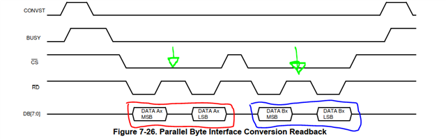
What I found odd is the following issue: As I'm using the EMIF interface to communicate with the ADC, this 16.bit ADC has the following time-schematic for a Byte Parallel Communication

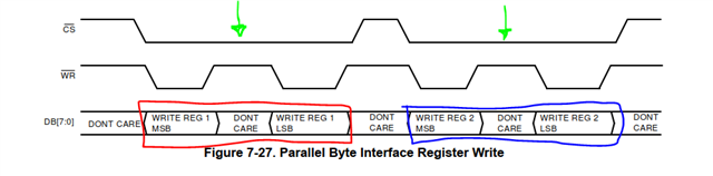
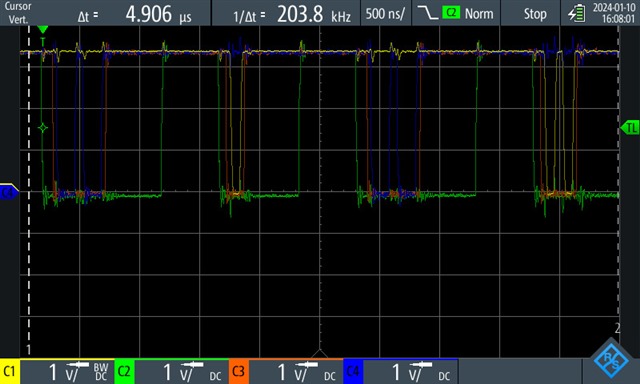
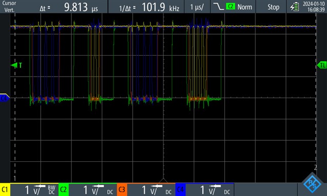
As you can see in the first picture, when using a 8 bit parallel communication, because the ADC is 16 bit, I have to read two times the ADC to read the whole conversion (it appears 4 read because it's a dual ADC and have 2 channels that are sampled simulataneously). The same with writing a register in the ADC, I have to write two times 8 bits to make a 16 bit frame. 

The difficulty is that in this time-schematics is that the Chip Select between same readings or writings remains low. I goes up and then goes low in the first picture when I want to read the conversion of the another channel. 

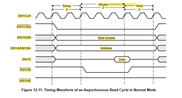
When I read the operation of the EMIF interface it has 3 phases, Setup, Strobe and Hold. At the end of the Hold period the CS goes up (inactive).

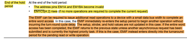
It says the following thing in orange: 

However, what I would need is that the Chip Select remains low after a first 8 bit reading before it reads another 8 bit reading to read the whole 16 bit frame of the adc. The same with the writing of the EMIF and the ADC. I would like to know if there is an option to after the Strobe period or hold period (OE is high-inactive) maintain the CS low-active and put the OE in low-active to do a dual reading without putting up the CS between the two readings.

I expect you could understand what I would like to know. I would be very grateful if you could help me.

Thank you in advance, have a nice day.

Pedro

  • We will have a look and get back to you by early next week.

  • Okey Vivek,

    I will wait for your answer. Thank you

  • Hi Pedro,

    As you know C28x is 16bit interface which means minimum access size is 16bit. On below query -

    However, what I would need is that the Chip Select remains low after a first 8 bit reading before it reads another 8 bit reading to read the whole 16 bit frame of the adc.

    If you configure the EMIF interface as 8bit (ASIZE = 0) and do a 16bit read/write from C28x then it should perform two back to back access without toggling the CS. Please see if that would work for this usecase.

    Regards,

    Vivek Singh

  • Hi Vivek,

    Thank you very much for your answer!. Following what you said, I did some tests to the EMIF of the TMS320F28388D. 

        Uint16 lectura16bits;
        Uint32 lectura32bits;
        //                                                                 configurarADC(tramaConfADC_NOSEQEN, 10, tramaFiltroPasoBajo, 8);
    
        EMIF_setAsyncDataBusWidth(EMIF1_BASE, EMIF_ASYNC_CS3_OFFSET,
                                      EMIF_ASYNC_DATA_WIDTH_16);
        pruebavariable16bits=0xF2F1;
        pruebavariable32bits=0xF2F11F2F;
    
        GPIO_writePin(GPIO_CS_EXT, 0);
        *punteroCS= pruebavariable16bits;
        GPIO_writePin(GPIO_CS_EXT, 1);
    
      GPIO_writePin(GPIO_CS_EXT, 0);
        lectura16bits=*punteroCS;
        GPIO_writePin(GPIO_CS_EXT, 1);
    
        GPIO_writePin(GPIO_CS_EXT, 0);
        *punteroCS= pruebavariable32bits;
        GPIO_writePin(GPIO_CS_EXT, 1);
    
        GPIO_writePin(GPIO_CS_EXT, 0);
        lectura32bits=*punteroCS;
        GPIO_writePin(GPIO_CS_EXT, 1);
    
        //LECTURA REGISTROS CONF. ADC
        //ConfADC=leerRegADC(lect_ConfADC, 8);
        //ConfADC=leerRegADC(lect_ConfADC, 16);
                                                                        /*  filtroADC=leerRegADC(lect_FPBADC,tamanobusdatos);
                                                                            rangoADCA=leerRegADC(lect_RangoADC_0_3_A,tamanobusdatos);
                                                                            rangoADCB=leerRegADC(lect_RangoADC_0_3_B,tamanobusdatos);*/
        EMIF_setAsyncDataBusWidth(EMIF1_BASE, EMIF_ASYNC_CS3_OFFSET,
                                  EMIF_ASYNC_DATA_WIDTH_8);                                //O PONER A 8 AUNQUE LUEGO PONER A 16 PARA EVITAR EL TURN-AROUND TIME
    
        GPIO_writePin(GPIO_CS_EXT, 0);
        *punteroCS= pruebavariable16bits;
        GPIO_writePin(GPIO_CS_EXT, 1);
    
        GPIO_writePin(GPIO_CS_EXT, 0);
        lectura16bits=*punteroCS;
        GPIO_writePin(GPIO_CS_EXT, 1);
    
        GPIO_writePin(GPIO_CS_EXT, 0);
        *punteroCS= pruebavariable32bits;
        GPIO_writePin(GPIO_CS_EXT, 1);
    
        GPIO_writePin(GPIO_CS_EXT, 0);
        lectura32bits=*punteroCS;
        GPIO_writePin(GPIO_CS_EXT, 1);
    

    As you can see from the code, I'm using the CS3 of the EMIF (asynchronous) and I will show you in the next pictures the following signals:

    - External CS: It's the external chip select managed as a GPIO. Color GREEN

    - EMIF CS3: It's the chip select of the EMIF interface of the microcontroller. Color RED

    - EMIF WEn: The write enable of the EMIF. Color BLUE

    - EMIF OEn: The output enable of the EMIF. Color YELLOW

    The pins I'm displaying are the following ones:

    As you can see, I'm using DB[0-7] to communicate with BYTE parallel with the ADC as the way I said in the last message

    What I did in the code was changing the ASIZE parameter with the "EMIF_setAsyncDataBusWidth" function. This code basically writes 2 variables of 16 bits and 32 bits and read it with the ASIZE of 16 bits and ASIZE of 8 bits.

    In the first picture I use ASIZE of 16bits.

    • If I write 16 bits ("pruebavariable16bits") the WEn(blue) goes down 2 times. Why?? I'm suppossing I'm writing with a 16 bit word memory, it would be only one cycle down. Then, if you see in the next operation, in the reading of the EMIF to a 16 bit variable ("lectura16bits") it shows the OEn only goes down one time.
    • If I write 32 bits ("pruebavariable32bits") the WEn(blue) goes down 2 times, the same as the 16bit variable!!!. Then, if you see in the next operation, in the reading of the EMIF to a 32 bit variable ("lectura32bits") it shows the OEn goes down two times.

    In the second picture, the ASIZE is 8 bits (the planned one to use in a byte parallel with 8 data buses with the ADC).

    • If I write 16 bits ("pruebavariable16bits") the WEn(blue) goes down 4 times!!. Is the same as the writting of the ASIZE of 16 bits but duplicated because the ASIZE is the half. If you see in the next operation, in the reading of the EMIF to a 16 bit variable ("lectura16bits") it shows the OEn goes down two times. It's right, two periods of reading to complete the 16 bit variable with two cicles of reading
    • If I write 32 bits ("pruebavariable32bits") the WEn(blue) goes down 2 times, the same as the 16bit variable!!!. If you see in the next operation, in the reading of the EMIF to a 32 bit variable ("lectura32bits") it shows the OEn goes down four times, what is the logical value.

    What I want to know is,  why in the writing operations the WEn makes 2 times the number of OEn that are made in the reading of a 16 bit variable. 

    I want to know why the writing operation of a 32 bit variable has the same cycles of WEn than a writing of a 16bit variable.

    As you know Vivak, I want to do that simple configuration to communicate with the ADC, that implies 2 readings operations and 2 writings operations with the ADC to write register of 16 bits with a 8 data bus. 

    I would very pleased if you could help me with this.

    Thank you in advance,

    Pedro

  • Can you share the definition of *punteroCS pointer.

  • Hi, Vivek.

    I give this pointer the direction of the CS3 that IS shown in the datasheets of the TMS320F28388D 

    The direction is the 0x0030 0000.

    Now I can't send you the exact code because I have my computer in job and I have finished my day. However, is the way I saw It was used the operations of write and read in some examples of EMIF of CCS, using a pointer to the direction of the Chip Select

    UPDATE:

    I write the code related to the pointer:

    #define CS3_DIRECCION  0x00300000
    Uint32 *punteroCS;
    
    punteroCS=(uint32_t*)CS3_DIRECCION;

  • You have defined the pointer as 32bit. I think that is why is it doing 32bit write. Please change it to 16bit.

    Vivek Singh

  • You were right Vivek, thank you very much!!!