This thread has been locked.

If you have a related question, please click the "Ask a related question" button in the top right corner. The newly created question will be automatically linked to this question.

TMS320F28377S: I have questions regarding the Interrupt Service Routine (ISR) in the provided 'ti' code and its connection to Analog-to-Digital Conversion (ADC).

Part Number: TMS320F28377S
Other Parts Discussed in Thread: C2000WARE

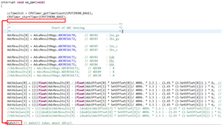
"I am involved in current control of an inverter, and I have created a code called 'daOut' to monitor internal variables. However, I have noticed significant differences in the current control characteristics when placing the 'daOut' code above and below the ADC register-related code inside the Interrupt Service Routine (ISR). In my understanding, I believe that the ADC-related code should take precedence at the beginning of the ISR. However, I have heard that some intentionally include dummy code before starting the ADC. Could you provide an explanation for this?

  • Hi,

    However, I have noticed significant differences in the current control characteristics when placing the 'daOut' code above and below the ADC register-related code

    Can you provide more details on the differences?

    Thanks

    Aswin

  • Thank you for your response.

    "I am aware that to read accurate ADCResults, I need to secure the Sample and Hold time (tSH) and Latch time (tLAT). In the specifications I am currently using, tSH+tLAT is 425ns. Therefore, I conducted three experiments using DELAY codes before reading the ADCResult values.

    1. Without any delay
    2. With a delay of 550ns (sufficient time secured)
    3. With a delay of 800ns (more time secured than Case 2)

    I know that without securing tSH+tLAT, reading ADCResults retrieves the existing values. Indeed, Cases 1 and 2 show a difference of one sampling. However, the strange aspect is Case 3. If tSH+tLAT is secured, ADCResults should be the same in Cases 2 and 3, but the values are different. In Case 3, it appears that the sampling delay of ADCResults is less than in Case 2. What could be the reason for this phenomenon?"

    Thanks
    Deokyong

  • Hello Deokyong,

    I'm sorry, it's not clear to me the exact circumstance for the issue. Can you show me your code (you can exclude any proprietary info if needed)? Where is this delay being added? It may be the case that it's causing an interrupt overflow for the ADC, depending on its location. Are you using an example ADC ISR provided by a TI example (if so, which one so I can refer to it)?

    In Case 3, it appears that the sampling delay of ADCResults is less than in Case 2.

    Can you clarify, are you saying the delay is not working properly or the ADC result itself is less than expected?

  • Thank you for your response.

    I'm using ti example ADC ISR.
    CC ISR is also used to control the inverter current, and both ISRs are synchronized to the up-down count of ePWM1.
    For current control, CC ISR must read the ADCResults value.
    Here, in order to secure the ADC's samp and hold time and latch time, a delay is inserted at the first point of CC ISR start.
  • I'm using ti example ADC ISR.

    There are 14 ADC examples for this device, you need to tell me which one you're referring to. What did you change from the example to your own project?

    CC ISR is also used to control the inverter current, and both ISRs are synchronized to the up-down count of ePWM1.

    From this I interpret that you're only using the ePWM to trigger the ISRs, not the ADC SOCs, is that correct?

    Here, in order to secure the ADC's samp and hold time and latch time, a delay is inserted at the first point of CC ISR start.

    Have you verified that there are no overflows by checking the ADCINTOVF and ADCSOCOVF1 registers?

  • The ISR is synchronized to ePWM and begins reading ADCResults values ​​as the ISR starts.
    Are ADC SOCs separate from ISR? I understand that when the ISR is triggered, the ADC SOCs also kick in.
    Is what I know wrong? Also, can you explain what overflows are?
  • Hello,

    Please share your code or which exact example you're using, I cannot provide much support if I can't see what you're doing. I need to see how your peripherals are configured, how the interrupts are set, the content of the ISRs, etc.

  • This is Adc code.

    //###########################################################################
    //
    // FILE:   F2837xS_Adc.c
    //
    // TITLE:  F2837xS Adc Support Functions.
    //
    //###########################################################################
    // $TI Release: F2837xS Support Library v210 $
    // $Release Date: Tue Nov  1 15:35:23 CDT 2016 $
    // $Copyright: Copyright (C) 2014-2016 Texas Instruments Incorporated -
    //             http://www.ti.com/ ALL RIGHTS RESERVED $
    //###########################################################################
    
    //
    // Included Files
    //
    #include "F2837xS_device.h"
    #include "F2837xS_Examples.h"
    
    
    void InitAdc(void)
    {
        Uint16 acqps = 19, tempsensor_acqps = 139; //temperature sensor needs at least 700ns
    
    
        EALLOW;
    
        AdcaRegs.ADCCTL2.bit.PRESCALE = 6; //set ADCCLK divider to /4
        AdcSetMode(ADC_ADCA, ADC_BITRESOLUTION_12BIT, ADC_SIGNALMODE_SINGLE);
        AdcaRegs.ADCCTL1.bit.INTPULSEPOS = 1;   // Set pulse positions to late
        AdcaRegs.ADCCTL1.bit.ADCPWDNZ = 1;      //power up the ADC
    
    
        AdcbRegs.ADCCTL2.bit.PRESCALE = 6; //set ADCCLK divider to /4
        AdcSetMode(ADC_ADCB, ADC_BITRESOLUTION_12BIT, ADC_SIGNALMODE_SINGLE);
        AdcbRegs.ADCCTL1.bit.INTPULSEPOS = 1;   // Set pulse positions to late
        AdcbRegs.ADCCTL1.bit.ADCPWDNZ = 1;    //power up the ADC
    
    
        AdccRegs.ADCCTL2.bit.PRESCALE = 6; //set ADCCLK divider to /4
        AdcSetMode(ADC_ADCC, ADC_BITRESOLUTION_12BIT, ADC_SIGNALMODE_SINGLE);
        AdccRegs.ADCCTL1.bit.INTPULSEPOS = 1;   // Set pulse positions to late
        AdccRegs.ADCCTL1.bit.ADCPWDNZ = 1;    //power up the ADC
    
    
        AdcdRegs.ADCCTL2.bit.PRESCALE = 6; //set ADCCLK divider to /4
        AdcSetMode(ADC_ADCD, ADC_BITRESOLUTION_12BIT, ADC_SIGNALMODE_SINGLE);
        AdcdRegs.ADCCTL1.bit.INTPULSEPOS = 1;   // Set pulse positions to late
        AdcdRegs.ADCCTL1.bit.ADCPWDNZ = 1;    //power up the ADC
    
    
        AdcaRegs.ADCSOCPRICTL.bit.SOCPRIORITY = 0x0f;
        acqps = 14 + AdcaRegs.ADCCTL2.bit.RESOLUTION * 49; // 75ns for 12bit mode, 320ns for 16bit mode
    
        //Select the channels to convert and end of conversion flag
        AdcaRegs.ADCSOC0CTL.bit.CHSEL = 0;      //SOC0 will convert pin A0
        AdcaRegs.ADCSOC0CTL.bit.ACQPS = acqps;  //sample window is 14 SYSCLK cycles
        AdcaRegs.ADCSOC0CTL.bit.TRIGSEL = 5;    //trigger on ePWM1 SOCA/C
    
        AdcaRegs.ADCSOC1CTL.bit.CHSEL = 1;      //SOC1 will convert pin A1
        AdcaRegs.ADCSOC1CTL.bit.ACQPS = acqps;  //sample window is 14 SYSCLK cycles
        AdcaRegs.ADCSOC1CTL.bit.TRIGSEL = 5;    //trigger on ePWM1 SOCA/C
    
        AdcaRegs.ADCSOC2CTL.bit.CHSEL = 2;      //SOC2 will convert pin A2
        AdcaRegs.ADCSOC2CTL.bit.ACQPS = acqps;  //sample window is 14 SYSCLK cycles
        AdcaRegs.ADCSOC2CTL.bit.TRIGSEL = 5;    //trigger on ePWM1 SOCA/C
    
        AdcaRegs.ADCSOC3CTL.bit.CHSEL = 3;      //SOC3 will convert pin A3
        AdcaRegs.ADCSOC3CTL.bit.ACQPS = acqps;  //sample window is 14 SYSCLK cycles
        AdcaRegs.ADCSOC3CTL.bit.TRIGSEL = 5;    //trigger on ePWM1 SOCA/C
    
        AdcaRegs.ADCSOC4CTL.bit.CHSEL = 4;      //SOC4 will convert pin A4
        AdcaRegs.ADCSOC4CTL.bit.ACQPS = acqps;  //sample window is 14 SYSCLK cycles
        AdcaRegs.ADCSOC4CTL.bit.TRIGSEL = 5;    //trigger on ePWM1 SOCA/C
    
        AdcaRegs.ADCSOC5CTL.bit.CHSEL = 5;      //SOC5 will convert pin A5
        AdcaRegs.ADCSOC5CTL.bit.ACQPS = acqps;  //sample window is 14 SYSCLK cycles
        AdcaRegs.ADCSOC5CTL.bit.TRIGSEL = 5;    //trigger on ePWM1 SOCA/C
    
        AdcaRegs.ADCSOC6CTL.bit.CHSEL = 13;      //SOC6 will convert pin TEMP SENSOR
        AdcaRegs.ADCSOC6CTL.bit.ACQPS = tempsensor_acqps;  //sample window is 100 SYSCLK cycles
        AdcaRegs.ADCSOC6CTL.bit.TRIGSEL = 5;    //trigger on ePWM1 SOCA/C
    
    
        //    AdcaRegs.ADCINTSEL1N2.bit.INT1SEL = 0; //end of SOC0 will set INT1 flag
        //    AdcaRegs.ADCINTSEL1N2.bit.INT1E = 1;   //enable INT1 flag
        //    AdcaRegs.ADCINTFLGCLR.bit.ADCINT1 = 1; //make sure INT1 flag is cleared
    
        // Adc B module :
        //Select the channels to convert and end of conversion flag
        AdcbRegs.ADCSOC0CTL.bit.CHSEL = 0;      //SOC0 will convert pin B0
        AdcbRegs.ADCSOC0CTL.bit.ACQPS = acqps;  //sample window is 14 SYSCLK cycles
        AdcbRegs.ADCSOC0CTL.bit.TRIGSEL = 5;    //trigger on ePWM1 SOCA/C
    
        AdcbRegs.ADCSOC1CTL.bit.CHSEL = 1;      //SOC1 will convert pin B1
        AdcbRegs.ADCSOC1CTL.bit.ACQPS = acqps;  //sample window is 14 SYSCLK cycles
        AdcbRegs.ADCSOC1CTL.bit.TRIGSEL = 5;    //trigger on ePWM1 SOCA/C
    
        AdcbRegs.ADCSOC2CTL.bit.CHSEL = 2;      //SOC2 will convert pin B2
        AdcbRegs.ADCSOC2CTL.bit.ACQPS = acqps;  //sample window is 14 SYSCLK cycles
        AdcbRegs.ADCSOC2CTL.bit.TRIGSEL = 5;    //trigger on ePWM1 SOCA/C
    
        AdcbRegs.ADCSOC3CTL.bit.CHSEL = 3;      //SOC3 will convert pin B3
        AdcbRegs.ADCSOC3CTL.bit.ACQPS = acqps;  //sample window is 14 SYSCLK cycles
        AdcbRegs.ADCSOC3CTL.bit.TRIGSEL = 5;    //trigger on ePWM1 SOCA/C
    
        AdcbRegs.ADCSOC4CTL.bit.CHSEL = 4;      //SOC4 will convert pin B4
        AdcbRegs.ADCSOC4CTL.bit.ACQPS = acqps;  //sample window is 14 SYSCLK cycles
        AdcbRegs.ADCSOC4CTL.bit.TRIGSEL = 5;    //trigger on ePWM1 SOCA/C
    
        AdcbRegs.ADCSOC5CTL.bit.CHSEL = 5;      //SOC5 will convert pin B5
        AdcbRegs.ADCSOC5CTL.bit.ACQPS = acqps;  //sample window is 14 SYSCLK cycles
        AdcbRegs.ADCSOC5CTL.bit.TRIGSEL = 5;    //trigger on ePWM1 SOCA/C
    
        // Adc C module :
        // Select the channels to convert and end of conversion flag
        AdccRegs.ADCSOC0CTL.bit.CHSEL = 14;      //SOC0 will convert pin 14
        AdccRegs.ADCSOC0CTL.bit.ACQPS = acqps;  //sample window is 14 SYSCLK cycles
        AdccRegs.ADCSOC0CTL.bit.TRIGSEL = 5;    //trigger on ePWM1 SOCA/C
    
        AdccRegs.ADCSOC1CTL.bit.CHSEL = 15;      //SOC1 will convert pin 15
        AdccRegs.ADCSOC1CTL.bit.ACQPS = acqps;  //sample window is 14 SYSCLK cycles
        AdccRegs.ADCSOC1CTL.bit.TRIGSEL = 5;    //trigger on ePWM1 SOCA/C
    
        AdccRegs.ADCSOC2CTL.bit.CHSEL = 2;      //SOC2 will convert pin C2
        AdccRegs.ADCSOC2CTL.bit.ACQPS = acqps;  //sample window is 14 SYSCLK cycles
        AdccRegs.ADCSOC2CTL.bit.TRIGSEL = 5;    //trigger on ePWM1 SOCA/C
    
        AdccRegs.ADCSOC3CTL.bit.CHSEL = 3;      //SOC3 will convert pin C3
        AdccRegs.ADCSOC3CTL.bit.ACQPS = acqps;  //sample window is 14 SYSCLK cycles
        AdccRegs.ADCSOC3CTL.bit.TRIGSEL = 5;    //trigger on ePWM1 SOCA/C
    
        AdccRegs.ADCSOC4CTL.bit.CHSEL = 4;      //SOC4 will convert pin C4
        AdccRegs.ADCSOC4CTL.bit.ACQPS = acqps;  //sample window is 14 SYSCLK cycles
        AdccRegs.ADCSOC4CTL.bit.TRIGSEL = 5;    //trigger on ePWM1 SOCA/C
    
        AdccRegs.ADCSOC5CTL.bit.CHSEL = 5;      //SOC5 will convert pin C5
        AdccRegs.ADCSOC5CTL.bit.ACQPS = acqps;  //sample window is 14 SYSCLK cycles
        AdccRegs.ADCSOC5CTL.bit.TRIGSEL = 5;    //trigger on ePWM1 SOCA/C
    
        // Adc D module :
        // Select the channels to convert and end of conversion flag
        AdcdRegs.ADCSOC0CTL.bit.CHSEL = 0;      //SOC0 wi   ll convert pin D0
        AdcdRegs.ADCSOC0CTL.bit.ACQPS = acqps*2;  //sample window is 14 SYSCLK cycles
        AdcdRegs.ADCSOC0CTL.bit.TRIGSEL = 5;    //trigger on ePWM1 SOCA/C
    
        AdcdRegs.ADCSOC1CTL.bit.CHSEL = 1;      //SOC1 will convert pin D1
        AdcdRegs.ADCSOC1CTL.bit.ACQPS = acqps;  //sample window is 14 SYSCLK cycles
        AdcdRegs.ADCSOC1CTL.bit.TRIGSEL = 5;    //trigger on ePWM1 SOCA/C
    
        AdcdRegs.ADCSOC2CTL.bit.CHSEL = 2;      //SOC2 will convert pin D2
        AdcdRegs.ADCSOC2CTL.bit.ACQPS = acqps;  //sample window is 14 SYSCLK cycles
        AdcdRegs.ADCSOC2CTL.bit.TRIGSEL = 5;    //trigger on ePWM1 SOCA/C
    
        AdcdRegs.ADCSOC3CTL.bit.CHSEL = 3;      //SOC3 will convert pin D3
        AdcdRegs.ADCSOC3CTL.bit.ACQPS = acqps;  //sample window is 14 SYSCLK cycles
        AdcdRegs.ADCSOC3CTL.bit.TRIGSEL = 5;    //trigger on ePWM1 SOCA/C
    
        AdcdRegs.ADCSOC4CTL.bit.CHSEL = 4;      //SOC4 will convert pin D4
        AdcdRegs.ADCSOC4CTL.bit.ACQPS = acqps;  //sample window is 14 SYSCLK cycles
        AdcdRegs.ADCSOC4CTL.bit.TRIGSEL = 5;    //trigger on ePWM1 SOCA/C
    
        AdcdRegs.ADCSOC5CTL.bit.CHSEL = 5;      //SOC5 will convert pin D5
        AdcdRegs.ADCSOC5CTL.bit.ACQPS = acqps;  //sample window is 14 SYSCLK cycles
        AdcdRegs.ADCSOC5CTL.bit.TRIGSEL = 5;    //trigger on ePWM1 SOCA/C
    
        EDIS;
    
        DELAY_US(1000);    //delay for 1ms to allow ADC time to power up
    
    }
    
    
    //
    // AdcSetMode - Set the resolution and signalmode for a given ADC. This will
    //              ensure that the correct trim is loaded.
    //
    void AdcSetMode(Uint16 adc, Uint16 resolution, Uint16 signalmode)
    {
        Uint16 adcOffsetTrimOTPIndex; //index into OTP table of ADC offset trims
        Uint16 adcOffsetTrim;         //temporary ADC offset trim
    
        //
        //re-populate INL trim
        //
        CalAdcINL(adc);
    
        if(0xFFFF != *((Uint16*)GetAdcOffsetTrimOTP))
        {
            //
            //offset trim function is programmed into OTP, so call it
            //
    
            //
            //calculate the index into OTP table of offset trims and call
            //function to return the correct offset trim
            //
            adcOffsetTrimOTPIndex = 4*adc + 2*resolution + 1*signalmode;
            adcOffsetTrim = (*GetAdcOffsetTrimOTP)(adcOffsetTrimOTPIndex);
        }
        else
        {
            //
            //offset trim function is not populated, so set offset trim to 0
            //
            adcOffsetTrim = 0;
        }
    
        //
        //Apply the resolution and signalmode to the specified ADC.
        //Also apply the offset trim and, if needed, linearity trim correction.
        //
        switch(adc)
        {
            case ADC_ADCA:
                AdcaRegs.ADCCTL2.bit.RESOLUTION = resolution;
                AdcaRegs.ADCCTL2.bit.SIGNALMODE = signalmode;
                AdcaRegs.ADCOFFTRIM.all = adcOffsetTrim;
                if(ADC_BITRESOLUTION_12BIT == resolution)
                {
                    //
                    //12-bit linearity trim workaround
                    //
                    AdcaRegs.ADCINLTRIM1 &= 0xFFFF0000;
                    AdcaRegs.ADCINLTRIM2 &= 0xFFFF0000;
                    AdcaRegs.ADCINLTRIM4 &= 0xFFFF0000;
                    AdcaRegs.ADCINLTRIM5 &= 0xFFFF0000;
                }
            break;
            case ADC_ADCB:
                AdcbRegs.ADCCTL2.bit.RESOLUTION = resolution;
                AdcbRegs.ADCCTL2.bit.SIGNALMODE = signalmode;
                AdcbRegs.ADCOFFTRIM.all = adcOffsetTrim;
                if(ADC_BITRESOLUTION_12BIT == resolution)
                {
                    //
                    //12-bit linearity trim workaround
                    //
                    AdcbRegs.ADCINLTRIM1 &= 0xFFFF0000;
                    AdcbRegs.ADCINLTRIM2 &= 0xFFFF0000;
                    AdcbRegs.ADCINLTRIM4 &= 0xFFFF0000;
                    AdcbRegs.ADCINLTRIM5 &= 0xFFFF0000;
                }
            break;
            case ADC_ADCC:
                AdccRegs.ADCCTL2.bit.RESOLUTION = resolution;
                AdccRegs.ADCCTL2.bit.SIGNALMODE = signalmode;
                AdccRegs.ADCOFFTRIM.all = adcOffsetTrim;
                if(ADC_BITRESOLUTION_12BIT == resolution)
                {
                    //
                    //12-bit linearity trim workaround
                    //
                    AdccRegs.ADCINLTRIM1 &= 0xFFFF0000;
                    AdccRegs.ADCINLTRIM2 &= 0xFFFF0000;
                    AdccRegs.ADCINLTRIM4 &= 0xFFFF0000;
                    AdccRegs.ADCINLTRIM5 &= 0xFFFF0000;
                }
            break;
            case ADC_ADCD:
                AdcdRegs.ADCCTL2.bit.RESOLUTION = resolution;
                AdcdRegs.ADCCTL2.bit.SIGNALMODE = signalmode;
                AdcdRegs.ADCOFFTRIM.all = adcOffsetTrim;
                if(ADC_BITRESOLUTION_12BIT == resolution)
                {
                    //
                    //12-bit linearity trim workaround
                    //
                    AdcdRegs.ADCINLTRIM1 &= 0xFFFF0000;
                    AdcdRegs.ADCINLTRIM2 &= 0xFFFF0000;
                    AdcdRegs.ADCINLTRIM4 &= 0xFFFF0000;
                    AdcdRegs.ADCINLTRIM5 &= 0xFFFF0000;
                }
            break;
        }
    }
    
    //
    // CalAdcINL - Loads INL trim values from OTP into the trim registers of the
    //             specified ADC. Use only as part of AdcSetMode function, since
    //             linearity trim correction is needed for some modes.
    //
    void CalAdcINL(Uint16 adc)
    {
        switch(adc)
        {
            case ADC_ADCA:
                if(0xFFFF != *((Uint16*)CalAdcaINL))
                {
                    //
                    //trim function is programmed into OTP, so call it
                    //
                    (*CalAdcaINL)();
                }
                else
                {
                    //
                    //do nothing, no INL trim function populated
                    //
                }
                break;
            case ADC_ADCB:
                if(0xFFFF != *((Uint16*)CalAdcbINL))
                {
                    //
                    //trim function is programmed into OTP, so call it
                    //
                    (*CalAdcbINL)();
                }
                else
                {
                    //
                    //do nothing, no INL trim function populated
                    //
                }
                break;
            case ADC_ADCC:
                if(0xFFFF != *((Uint16*)CalAdccINL))
                {
                    //
                    //trim function is programmed into OTP, so call it
                    //
                    (*CalAdccINL)();
                }
                else
                {
                    //
                    //do nothing, no INL trim function populated
                    //
                }
                break;
            case ADC_ADCD:
                if(0xFFFF != *((Uint16*)CalAdcdINL))
                {
                    //
                    //trim function is programmed into OTP, so call it
                    //
                    (*CalAdcdINL)();
                }
                else
                {
                    //
                    //do nothing, no INL trim function populated
                    //
                }
                break;
        }
    }
    
    //
    // End of file
    //
    

    And, this is ISR code.

    interrupt void cc_isr(void)
    {
    
        //ccTimeInit = CPUTimer_getTimerCount(CPUTIMER0_BASE);
        //CPUTimer_startTimer(CPUTIMER0_BASE);
        //daOut();  // daOut() takes about 10[us].
        DELAY_US(0.55);
        /*------------------------------------------------------------------*/
        /*                         Start of ADC Sensing                     */
        /*------------------------------------------------------------------*/
        AdcResults[0] = AdcaResultRegs.ADCRESULT0;     // ADC01     : Ias_gs
        AdcResults[2] = AdcaResultRegs.ADCRESULT2;     // ADC03     : Ibs_gs
    
        AdcResults[4] = AdcaResultRegs.ADCRESULT4;     // ADC05     : Ias_c
        AdcResults[6] = AdccResultRegs.ADCRESULT0;     // ADC07     : Ibs_c
    
        AdcResults[1] = AdcaResultRegs.ADCRESULT1;     // ADC02     : Eab
        AdcResults[3] = AdcaResultRegs.ADCRESULT3;     // ADC04     : Ebc
        AdcResults[5] = AdcaResultRegs.ADCRESULT5;     // ADC06     : Vdc
        //AdcResults[7] = AdccResultRegs.ADCRESULT1;     // ADC08     : X
        AdcResults[8] = AdccResultRegs.ADCRESULT2;     // ADC09     : X
        //AdcResults[9] = AdccResultRegs.ADCRESULT3;     // ADC10     : X
    
        AdcValues[0] = ((((float)AdcResults[0] - (float)AdcOffset[0] * SetOffset[0])/ 4096. * 3.3 ) - (1.65 * (1-SetOffset[0])) ) * 6;  // ADC01
        AdcValues[1] = ((((float)AdcResults[1] - (float)AdcOffset[1] * SetOffset[1])/ 4096. * 3.3 ) - (1.65 * (1-SetOffset[1])) ) * 6;  // ADC02
        AdcValues[2] = ((((float)AdcResults[2] - (float)AdcOffset[2] * SetOffset[2])/ 4096. * 3.3 ) - (1.65 * (1-SetOffset[2])) ) * 6;  // ADC03
        AdcValues[3] = ((((float)AdcResults[3] - (float)AdcOffset[3] * SetOffset[3])/ 4096. * 3.3 ) - (1.65 * (1-SetOffset[3])) ) * 6;  // ADC04
        AdcValues[4] = ((((float)AdcResults[4] - (float)AdcOffset[4] * SetOffset[4])/ 4096. * 3.3 ) - (1.65 * (1-SetOffset[4])) ) * 6;  // ADC05
        AdcValues[5] = ((((float)AdcResults[5] - (float)AdcOffset[5] * SetOffset[5])/ 4096. * 3.3 ) - (1.65 * (1-SetOffset[5])) ) * 6;  // ADC06
        AdcValues[6] = ((((float)AdcResults[6] - (float)AdcOffset[6] * SetOffset[6])/ 4096. * 3.3 ) - (1.65 * (1-SetOffset[6])) ) * 6;  // ADC07
        //AdcValues[7] = ((((double)AdcResults[7] - (double)AdcOffset[7] * SetOffset[7])/ 4096. * 3.3 ) - (1.65 * (1-SetOffset[7])) ) * 6;  // ADC08
        AdcValues[8] = ((((float)AdcResults[8] - (float)AdcOffset[8] * SetOffset[8])/ 4096. * 3.3 ) - (1.65 * (1-SetOffset[8])) ) * 6;  // ADC09
        //AdcValues[9] = ((((double)AdcResults[9] - (double)AdcOffset[9] * SetOffset[9])/ 4096. * 3.3 ) - (1.65 * (1-SetOffset[9])) ) * 6;  // ADC10
    
        // <-- ADC variable calculation
        /*Ias_gs_test = AdcValues[0] * AdcScale[0];    // A-phase Grid-side Current
        Ibs_gs_test = AdcValues[2] * AdcScale[2];    // B-phase Grid-side Current
        Ics_gs_test = -(Ias_gs_test + Ibs_gs_test);  // C-phase Grid-side Current
        Ias_c_test = AdcValues[4] * AdcScale[4];     // A-phase Capacitor Current
        Ibs_c_test = AdcValues[6] * AdcScale[6];     // B-phase Capacitor Current
        Ics_c_test = -(Ias_c_test + Ibs_c_test);     // B-phase Capacitor Current
        Eab_test = AdcValues[1] * AdcScale[1];       // AB line to line Voltage
        Ebc_test = AdcValues[3] * AdcScale[3];       // BC line to line Voltage
        Eca_test = -(Eab_test + Ebc_test);           // CA line to line Voltage
        Vdc_test = AdcValues[5] * AdcScale[5];       // DC-link Voltage*/
    
        Controller.Ias_gs = AdcValues[0] * AdcScale[0];                // A-phase Grid-side Current
        Controller.Ibs_gs = AdcValues[2] * AdcScale[2];                // B-phase Grid-side Current
        Controller.Ics_gs = AdcValues[8] * AdcScale[8];//-(Controller.Ias_gs + Controller.Ibs_gs);  // C-phase Grid-side Current
        Controller.Ias_c = AdcValues[4] * AdcScale[4];                 // A-phase Capacitor Current
        Controller.Ibs_c = AdcValues[6] * AdcScale[6];                 // B-phase Capacitor Current
        Controller.Ics_c = -(Controller.Ias_c + Controller.Ibs_c);     // C-phase Capacitor Current
        GRID_AC.Eab = AdcValues[1] * AdcScale[1];                      // AB line to line Voltage
        GRID_AC.Ebc = AdcValues[3] * AdcScale[3];                      // BC line to line Voltage
        GRID_AC.Eca = -(GRID_AC.Eab + GRID_AC.Ebc);                    // CA line to line Voltage
        Controller.Vdc = AdcValues[5] * AdcScale[5];                   // DC-link Voltage
    
        /*------------------------------------------------------------------*/
        /*                         End of ADC Sensing                       */
        /*------------------------------------------------------------------*/
    
        /*------------------------------------------------------------------*/
        /*                         Start of Software Fault                  */
        /*------------------------------------------------------------------*/
    
        if(fabs(Controller.Ias_gs) > OC_Set_line)        Faults.SW_Prot.bit.OC_Ias = 1;
        if(fabs(Controller.Ibs_gs) > OC_Set_line)        Faults.SW_Prot.bit.OC_Ibs = 1;
        if(fabs(Controller.Ics_gs) > OC_Set_line)        Faults.SW_Prot.bit.OC_Ics = 1;
        if(fabs(GRID_AC.Eab) > OV_Set_line2line)         Faults.SW_Prot.bit.OV_Eab = 1;
        if(fabs(GRID_AC.Ebc) > OV_Set_line2line)         Faults.SW_Prot.bit.OV_Ebc = 1;
        if(fabs(Controller.Vdc) > OV_Set_DClink)         Faults.SW_Prot.bit.OV_Vdc = 1;
    
        if(Faults.SW_Prot.all){
        faultManage();
        checkHWFault();
        }
    
        /*------------------------------------------------------------------*/
        /*                         End of Software Fault                    */
        /*------------------------------------------------------------------*/
    
    //    // <-- Enable Signal
    
        if(Flags.EnableCnv == 1 && Flags.EnableCnv_Old == 0) {
    
            Flags.EnableGD2 = 1;
            //do something --> Flag_CCont = 1;
            Flags.EnableCnv_Old = 1;
        }
        if(Flags.EnableCnv == 0 && Flags.EnableCnv_Old == 1) {
           // Flags.EnableGD2 = 0;
            //do something --> Flag_VdcPCont = 0, Flag_BalCont = 0, Flag_CCont = 0;
            //do something --> Flag_StartDAB = 0, Flag_ControlDAB = 0;
            Flags.EnableCnv_Old = 0;
        }
    
        if(Flags.EnableInv == 1 && Flags.EnableInv_Old == 0) {
            Flags.EnableGD1 = 1;
            //do something --> Flag_CCont = 1;
            Flags.EnableInv_Old = 1;
        }
        if(Flags.EnableInv == 0 && Flags.EnableInv_Old == 1) {
         //   Flags.EnableGD1 = 0;
            //do something --> Flag_VdcPCont = 0, Flag_BalCont = 0, Flag_CCont = 0;
            //do something --> Flag_StartDAB = 0, Flag_ControlDAB = 0;
            Flags.EnableInv_Old = 0;
    
        }
    
        /*------------------------------------------------------------------*/
        /*                         User Code Start                          */
        /*------------------------------------------------------------------*/
    
        if(Flags.PLL_Start == 1){
    
            GRID_Update(&GRID_AC);
            Detector_Update(&Controller);
            tEqe_err = GRID_AC.Eqep / GRID_AC.Epeakp;
            PLL_Control(&GRID_AC_PLL, tEqe_err);
    
            GRID_AC.Thetae = GRID_AC_PLL.Thetae;
            GRID_AC.We = GRID_AC_PLL.We;
    
            }
    
        if(Flags.Detector_Start == 1){
    
            Detector_Update(&Controller);
            Controller.Thetae = GRID_AC_PLL.Thetae;
            Controller.We = GRID_AC_PLL.We;
            Controller.Ede = GRID_AC.Edep;
            Controller.Eqe = GRID_AC.Eqep;
            Controller.Eds = GRID_AC.Edsp;
            Controller.Eqs = GRID_AC.Eqsp;
            }
    
        if(Flags.Run_zero == 1 && (GRID_AC.Eab < 1 && GRID_AC.Eab > -1)){
    
            Flags.Run = 1;
            }
    
        if(Flags.Run == 1){
    
            Current_Controller(&Controller);
            Flags.StartInverter = 1;
            //Energy_Controller(&Controller);
    
            }
    
        if(Flags.Run == 1 && Flags.Stop == 1){
    
            GaCountA =0.; GaCountB =0.; GaCountC =0.;
            Flags.StartInverter = 0;
            Controller_Init(&Controller);
            Flags.Run_zero = 0;
            Flags.Run = 0;
            Flags.Stop = 0;
    
          }
    
        /*------------------------------------------------------------------*/
        /*                          User Code End                           */
        /*------------------------------------------------------------------*/
    
        // <-- Gating Counter Value Update
        // Inverter FLOAT to INT conversion
    
       GaCountA = (int)(SYS_CLK * Controller.TDuty_A);
       GaCountA = (GaCountA > PWMMaxCount) ? PWMMaxCount : ((GaCountA < 0) ? 0 : GaCountA);
       GaCountB = (int)(SYS_CLK * Controller.TDuty_B);
       GaCountB = (GaCountB > PWMMaxCount) ? PWMMaxCount : ((GaCountB < 0) ? 0 : GaCountB);
       GaCountC = (int)(SYS_CLK * Controller.TDuty_C);
       GaCountC = (GaCountC > PWMMaxCount) ? PWMMaxCount : ((GaCountC < 0) ? 0 : GaCountC);
    
        // ***** PWM1 ***** //
        EPwm1Regs.CMPA.bit.CMPA = GaCountA;
        EPwm2Regs.CMPA.bit.CMPA = GaCountB;
        EPwm3Regs.CMPA.bit.CMPA = GaCountC;
    
        // ***** PWM2 ***** //
        /*EPwm4Regs.CMPA.bit.CMPA= GaCountA2;
        EPwm5Regs.CMPA.bit.CMPA= GaCountB2;
        EPwm6Regs.CMPA.bit.CMPA= GaCountC2;*/
    
    
        // <-- PWM count reference mapping
        // EPwm1Regs.CMPA.bit.CMPA = PWM01_Count_Ref;
        // EPwm2Regs.CMPA.bit.CMPA = PWM02_Count_Ref;
        // EPwm3Regs.CMPA.bit.CMPA = PWM03_Count_Ref;
        // EPwm4Regs.CMPA.bit.CMPA = PWM04_Count_Ref;
        // EPwm5Regs.CMPA.bit.CMPA = PWM05_Count_Ref;
        // EPwm6Regs.CMPA.bit.CMPA = PWM06_Count_Ref;
        // EPwm7Regs.CMPA.bit.CMPA = PWM07_Count_Ref;
        // EPwm8Regs.CMPA.bit.CMPA = PWM08_Count_Ref;
        // EPwm9Regs.CMPA.bit.CMPA = PWM09_Count_Ref;
        // EPwm10Regs.CMPA.bit.CMPA = PWM10_Count_Ref;
        // EPwm11Regs.CMPA.bit.CMPA = PWM11_Count_Ref;
        // EPwm12Regs.CMPA.bit.CMPA = PWM12_Count_Ref;
        // PWM count reference mapping -->
    
    
    ///// <-- Gating Signal Enable
    /*
        if(Flags.Fault == 0 && Flags.Fault_Old == 0) {
            checkHWFault();
            if(Flags.EnableStart_Old == 0 && Flags.EnableStart == 1) {
                if(Flags.EnableGD1 == 1)    GpioDataRegs.GPCCLEAR.bit.GPIO69 = 1;               // GPIO69 = GD1_OEn
                else                GpioDataRegs.GPCSET.bit.GPIO69 = 1;
                if(Flags.EnableGD2 == 1)    GpioDataRegs.GPCCLEAR.bit.GPIO70 = 1;               // GPIO70 = GD2_OEn
                else                GpioDataRegs.GPCSET.bit.GPIO70 = 1;
                if(Flags.EnableGD3 == 1)    GpioDataRegs.GPCCLEAR.bit.GPIO74 = 1;               // GPIO74 = GD3_OEn
                else                GpioDataRegs.GPCSET.bit.GPIO74 = 1;
                if(Flags.EnableGD4 == 1)    GpioDataRegs.GPCCLEAR.bit.GPIO75 = 1;               // GPIO75 = GD4_OEn
                else                GpioDataRegs.GPCSET.bit.GPIO75 = 1;
    
                Flags.EnableStart_Old = 1;
            }
            if(Flags.EnableStart_Old == 1 && Flags.EnableStart == 0) {
                Flags.EnableGD1 = 0, GpioDataRegs.GPCSET.bit.GPIO69 = 1;
                Flags.EnableGD2 = 0, GpioDataRegs.GPCSET.bit.GPIO70 = 1;
                Flags.EnableGD3 = 0, GpioDataRegs.GPCSET.bit.GPIO74 = 1;
                Flags.EnableGD4 = 0, GpioDataRegs.GPCSET.bit.GPIO75 = 1;
                Flags.EnableStart_Old = 0;
            }
        } else {
            faultManage();
        }
        */
    
        if(Flags.Fault == 0 && Flags.Fault_Old == 0) {
               checkHWFault();
               if(Flags.StartInverter_old == 0 && Flags.StartInverter == 1) {Flags.EnableGD1 = 1;
                   if(Flags.EnableGD1 == 1)    GpioDataRegs.GPCCLEAR.bit.GPIO69 = 1;               // GPIO69 = GD1_OEn
                   else                GpioDataRegs.GPCSET.bit.GPIO69 = 1;
    
                   Flags.StartInverter_old = 1;
               }
               if(Flags.StartInverter_old == 1 && Flags.StartInverter == 0) {
                   Flags.EnableGD1 = 0, GpioDataRegs.GPCSET.bit.GPIO69 = 1;
                   Flags.StartInverter_old = 0;
               }
    
               if(Flags.StartCnverter_old == 0 && Flags.StartCnverter == 1) { Flags.EnableGD2 = 1;
                   if(Flags.EnableGD2 == 1)    GpioDataRegs.GPCCLEAR.bit.GPIO70 = 1;               // GPIO70 = GD2_OEn
                   else                GpioDataRegs.GPCSET.bit.GPIO70 = 1;
    
                   Flags.StartCnverter_old = 1;
               }
               if(Flags.StartCnverter_old == 1 && Flags.StartCnverter == 0) {
                   Flags.EnableGD2 = 0, GpioDataRegs.GPCSET.bit.GPIO70 = 1;
                   Flags.StartCnverter_old = 0;
                 }
           }
    
        else {
               faultManage();
           }
        ///// Gating Signal Enable -->
    
        // <-- Fault reset check
        if(Flags.Reset == 1) {
            checkHWFault();
            if(GpioDataRegs.GPBDAT.bit.GPIO53 == 0x1) {
                Flags.Fault = 0;
                Flags.Fault_Old = 0;
                Flags.Reset = 0;
                Fault_cnt=0;
            }
            else{
            Flags.Reset = 0;}
        }
    
        // Fault reset check -->
    
    
        // <-- LED code
        if(cc_cnt >= 5000U) {
            cc_cnt = 0;
            //GpioDataRegs.GPBTOGGLE.bit.GPIO48 = 1;       // LED0 - Red
            //GpioDataRegs.GPBTOGGLE.bit.GPIO49 = 1;       // LED1 -
            GpioDataRegs.GPBTOGGLE.bit.GPIO50 = 1;       // LED2 - Yellow
            //GpioDataRegs.GPBTOGGLE.bit.GPIO51 = 1;       // LED3 - Blue
        } else {
            cc_cnt++;
        }
    
        // LEC code -->
    
        // <-- Timer stop
        CPUTimer_stopTimer(CPUTIMER0_BASE);
        ccTimePresent = CPUTimer_getTimerCount(CPUTIMER0_BASE);
        ccTime_us = 1000000.*(float)SYS_CLK_PRD*(ccTimeInit - ccTimePresent);
        CPUTimer_reloadTimerCounter(CPUTIMER0_BASE);
        // Timer stop -->
    
     //   EPwm1Regs.ETCLR.bit.SOCA = 1; //clear SOCA flag
        EPwm1Regs.ETCLR.bit.INT = 1; //clear INT flag
        PieCtrlRegs.PIEACK.all = PIEACK_GROUP3;
    
    }
    /////////////////////////////////CC END/////////////////////////////////////////
    

    Here, I inserted a DELAY at the beginning of the ISR to secure the Sample and Hold time and LATCH time.

  • Hello,

    Your ISR seems to be extremely long without even the delay taken into account. Please read section 10.7.1 Interrupt Overflow in the ADC chapter of the reference manual to understand more about checking this. You can also refer to examples provided in C2000Ware_5_01_00_00\driverlib\f2837xs\examples\cpu1\adc that give a better idea on how to configure the ADC and its interrupts for certain use-cases. Interrupt overflows should be avoided to get more accurate ADC readings.

    In general, ISRs should be as short as possible since the intention is to use them for real-time programs, where interrupts happen and are handled fast.

  • I control with a sample period of 100 us, and the total execution time of my ISR is around 50 us, providing sufficient margin. My curiosity lies in reading the ADCResults values simultaneously with the start of the ISR. Considering the Samp and Hold time and LATCH time, I added a DELAY of approximately 550 ns, and in this case, the ADC appears to operate correctly (I referred to Section 10.12.). However, when I excessively add a DELAY of 1 us, the ADC reads values differently. If no DELAY is added, the ADC reads the existing data, as expected since Samp and Hold time + LATCH time (my specification is 400 ns) are not secured.

    summary)
    1. without DELAY, the ADC reads the existing data.

    2. When considering Samp and Hold time + LATCH time with a DELAY of around 550 ns, correct values are read.

    3. Adding a DELAY of 1 us or more causes the ADC to read values delayed compared to the ePWM's Up-Down Count point.

    I believe the results of 2 and 3 should be the same.

  • I control with a sample period of 100 us

    I see, I didn't see your ePWM configuration code so I thought you were triggering the ADC as fast as possible.

    2. When considering Samp and Hold time + LATCH time with a DELAY of around 550 ns, correct values are read.

    3. Adding a DELAY of 1 us or more causes the ADC to read values delayed compared to the ePWM's Up-Down Count point.

    I believe the results of 2 and 3 should be the same

    Are you running this program in Flash or RAM? Did you use the CPU timer or DELAY_US to create the delay (your screenshot is inconsistent with the code you provided)?

    For context, running from Flash will always be slower than running from RAM, so a delay function like DELAY_US will create a delay by burning cycles which takes longer in Flash (which could cause an interrupt overflow). However, using the CPU timer counts the ticks of a separate timer from the CPU, so it should work on Flash. You should also verify the delays that you're adding by toggling a GPIO or some external signal to verify the length between each ISR trigger. Let me know if you see consistent timing by doing this.