Other Parts Discussed in Thread: TMS320F28386D, C2000WARE
Hello,
I am trying to use TMS320F28377S MCBSP A port as an SPI slave and use DMA CH6 to receive data. Is DMA supported for MCBSP SPI slave on the TMS320F28377S? I notice the MCBSP register DRR1 does get the first 16-bit word in a transfer from the master but it seems like the DMA controller is not moving the data. I am using 16-bit words for data transfer. If I use a transfer size of 1 and burst size of 1 I will get a DMA interrupt but the data isn't read from DRR1.
Other key points
- I'm able to send and receive data on the TMS320F28377S over the MCBSP A SPI port as a slave using interrupts without DMA. This works fine.
- I am able to use the TMS320F28386D MCBSP B port as a SPI master with tx/rx DMA transfers. It works fine.
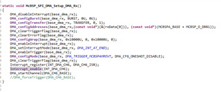
void main(void)
{
    //
    // Initialize device clock and peripherals
    //
    Device_init();

    GPIO_Setup();

    //
    // Initialize PIE and clear PIE registers. Disables CPU interrupts.
    //
    Interrupt_initModule();

    //
    // Initialize the PIE vector table with pointers to the shell Interrupt
    // Service Routines (ISR).
    //
    Interrupt_initVectorTable();

    McBSP_SPI_DMA_Setup();

    IER = 0x60;

    //
    // Enable Global Interrupt (INTM) and realtime interrupt (DBGM)
    //
    EINT;
    ERTM;

    while(true)
    {
        //Loop forever
    }
}
#include "driverlib.h"
#include "device.h"
#include <stdint.h>
#include <string.h>


#pragma DATA_SECTION(txData, "ramgs0");  // map the TX data to memory
#pragma DATA_SECTION(rxData, "ramgs0");  // map the RX data to memory


#define MCBSP_PING_PONG_SIZE                2
#define BURST                               1
//#define TRANSFER                          512
//#define TRANSFER                          5         //For Testing to See 5 uint16_t on the scope
#define TRANSFER                            1         //Transfer size of 1 causes an interrupt

volatile uint16_t txData[TRANSFER];
volatile uint16_t rxData[TRANSFER];

uint32_t base_mcbsp=MCBSPA_BASE;
uint32_t base_dma_tx=DMA_CH5_BASE;
uint32_t base_dma_rx=DMA_CH6_BASE;


//
// Define to select delay in clock cycles.
//
#define MCBSP_CYCLE_NOP0(n)  __asm(" RPT #(" #n ") || NOP")
#define MCBSP_CYCLE_NOP(n)   MCBSP_CYCLE_NOP0(n)


__interrupt void DMA_CH5_ISR();
__interrupt void DMA_CH6_ISR();

static void McBSP_SPI_DMA_Setup_McBSP()
{

    //
    // Reset FS generator, sample rate generator, transmitter, receiver.
    //
    McBSP_resetFrameSyncLogic(base_mcbsp);
    McBSP_resetSampleRateGenerator(base_mcbsp);
    McBSP_resetTransmitter(base_mcbsp);
    McBSP_resetReceiver(base_mcbsp);

    //
    // Set Rx sign-extension and justification mode.
    //
    McBSP_setRxSignExtension(base_mcbsp, MCBSP_RIGHT_JUSTIFY_FILL_ZERO);

    //
    // Enable clock stop mode.
    //
    McBSP_setClockStopMode(base_mcbsp, MCBSP_CLOCK_SPI_MODE_NO_DELAY);

    //
    // Set Rx & Tx delay to 0 cycle.
    //
    McBSP_setRxDataDelayBits(base_mcbsp, MCBSP_DATA_DELAY_BIT_0);
    McBSP_setTxDataDelayBits(base_mcbsp, MCBSP_DATA_DELAY_BIT_0);

    //
    // Set CLKX & FSX as inputs
    //
    McBSP_setTxClockSource(base_mcbsp, MCBSP_EXTERNAL_TX_CLOCK_SOURCE);
    McBSP_setTxFrameSyncSource(base_mcbsp, MCBSP_TX_EXTERNAL_FRAME_SYNC_SOURCE);

    //
    // Set Tx and Rx clock and frame-sync polarity.
    //
    McBSP_setTxFrameSyncPolarity(base_mcbsp, MCBSP_TX_FRAME_SYNC_POLARITY_LOW);
    McBSP_setTxClockPolarity(base_mcbsp, MCBSP_TX_POLARITY_RISING_EDGE);
    McBSP_setRxClockPolarity(base_mcbsp, MCBSP_RX_POLARITY_FALLING_EDGE);

    //
    // Initialize McBSP data length.
    //
    McBSP_setRxDataSize(base_mcbsp, MCBSP_PHASE_ONE_FRAME, MCBSP_BITS_PER_WORD_16, 0);
    McBSP_setTxDataSize(base_mcbsp, MCBSP_PHASE_ONE_FRAME, MCBSP_BITS_PER_WORD_16, 0);

    //
    // Set LSPCLK as input source for sample rate generator.
    //
    McBSP_setTxSRGClockSource(base_mcbsp, MCBSP_SRG_TX_CLOCK_SOURCE_LSPCLK);

    //
    // Set Divide down value for CLKG.
    //
    McBSP_setSRGDataClockDivider(base_mcbsp, 1);

    //
    // Enable Rx interrupt
    //
    //McBSP_enableRxInterrupt(base_mcbsp);

    //McBSP_enableTxInterrupt(base);
    //
    // Set no external clock sync for CLKG.
    //
    McBSP_disableSRGSyncFSR(base_mcbsp);

    //
    // Wait for CPU cycles equivalent to 2 SRG cycles-init delay.
    // Total cycles required = 2*(SYSCLK/LSPCLK). In this example
    // LSPCLK = SYSCLK/4.
    //
    MCBSP_CYCLE_NOP(8);

    //
    // Enable Sample rate generator and wait for at least 2 CLKG clock cycles.
    //
    McBSP_enableSampleRateGenerator(base_mcbsp);
    McBSP_enableFrameSyncLogic(base_mcbsp);

    //
    // Wait for CPU cycles equivalent to 2 CLKG cycles-init delay.
    // Total cycles required = 2*(SYSCLK/(LSPCLK/(1+CLKGDV_VAL))). In this
    // example LSPCLK = SYSCLK/4 and CLKGDV_VAL = 1.
    //
    MCBSP_CYCLE_NOP(16);

    //
    // Release Rx, Tx and frame-sync generator from reset.
    //
    McBSP_enableTransmitter(base_mcbsp);
    McBSP_enableReceiver(base_mcbsp);

    //
    // Wait for CPU cycles equivalent to 2 SRG cycles-init delay.
    // Total cycles required = 2*(SYSCLK/LSPCLK). In this example
    // LSPCLK = SYSCLK/4.
    //
    MCBSP_CYCLE_NOP(8);

    //Interrupt_register(INT_MCBSPA_RX, McBSP_SPI_Rx_Interrupt);
    //Interrupt_enable(INT_MCBSPA_RX);

}


static void McBSP_SPI_DMA_Setup_DMA_Tx()
{
    //
    // Configure DMA Channel 1 (16 - bit datasize).
    //
    DMA_disableInterrupt(base_dma_tx);

    //
    // Configure 1 word per burst.
    //
    DMA_configBurst(base_dma_tx, BURST, 0U, 0U);

    //
    // Configure 127 bursts per transfer.
    //
    DMA_configTransfer(base_dma_tx, TRANSFER, 1, 0);

    //
    // Src start address = buffer & dest start address = MCBSPA DXR
    //
    DMA_configAddresses(base_dma_tx, (const void*)(base_mcbsp + MCBSP_O_DXR1), (const void*)(&(txData[0])));

    //
    // Clear peripheral interrupt event flag.
    //
    DMA_clearTriggerFlag(base_dma_tx);

    //
    // Clear sync error flag.
    //
    DMA_clearErrorFlag(base_dma_tx);

    //
    // Configure wrap size to maximum to avoid wrapping.
    //
    DMA_configWrap(base_dma_tx, 0x10000U, 0, 0x10000U, 0);


    Interrupt_register(INT_DMA_CH5, DMA_CH5_ISR);

    //
    // Enable channel interrupt.
    //
    DMA_enableInterrupt(base_dma_tx);

    //
    // Interrupt at end of the transfer.
    //
    DMA_setInterruptMode(base_dma_tx, DMA_INT_AT_END);

    //
    // Enable selected peripheral trigger to start a DMA transfer on DMA
    // channel 1.
    //
    DMA_enableTrigger(base_dma_tx);

    //
    // Configure DMA trigger source as McBSPA Tx EVT.
    //
    //DMA_configMode(base_dma_tx, DMA_TRIGGER_MCBSPAMXEVT, DMA_CFG_ONESHOT_ENABLE);
    DMA_configMode(base_dma_tx, DMA_TRIGGER_MCBSPAMXEVT, DMA_CFG_ONESHOT_DISABLE);

    //
    // Clear any spurious Peripheral interrupts flags.
    //
    DMA_clearTriggerFlag(base_dma_tx);

    //
    // Enable interrupts in PIE block.
    //
    Interrupt_enable(INT_DMA_CH5);
}


static void McBSP_SPI_DMA_Setup_DMA_Rx()
{
    //
    // Configure DMA Channel 2 (16 - bit datasize).
    //
    DMA_disableInterrupt(base_dma_rx);

    //
    // Configure 1 word per burst.
    //
    DMA_configBurst(base_dma_rx, BURST, 0U, 0U);

    //
    // Configure 127 bursts per transfer.
    //
    DMA_configTransfer(base_dma_rx, TRANSFER, 0, 1);

    //
    // Dest start address = buffer & Src start address = MCBSPA DRR
    //
    DMA_configAddresses(base_dma_rx,(const void*)(&(rxData[0])), (const void*)(MCBSPA_BASE + MCBSP_O_DRR2));

    //
    // Clear peripheral interrupt event flag.
    //
    DMA_clearTriggerFlag(base_dma_rx);

    //
    // Clear sync error flag.
    //
    DMA_clearErrorFlag(base_dma_rx);

    //
    // Configure wrap size to maximum to avoid wrapping.
    //
    DMA_configWrap(base_dma_rx, 0x10000U, 0, 0x10000U, 0);


    Interrupt_register(INT_DMA_CH6, DMA_CH6_ISR);

    //
    // Enable channel interrupt.
    //
    DMA_enableInterrupt(base_dma_rx);

    //
    // Interrupt at end of the transfer.
    //
    DMA_setInterruptMode(base_dma_rx, DMA_INT_AT_END);

    //
    // Enable selected peripheral trigger to start a DMA transfer on DMA
    // channel 2.
    //
    DMA_enableTrigger(base_dma_rx);

    //
    // Configure DMA trigger source as McBSPA Tx EVT.
    //
    //DMA_configMode(base_dma_rx, DMA_TRIGGER_MCBSPAMREVT, 0);
    DMA_configMode(base_dma_rx, DMA_TRIGGER_MCBSPAMREVT, DMA_CFG_ONESHOT_DISABLE);
    //DMA_configMode(base_dma_rx, DMA_TRIGGER_MCBSPAMREVT, DMA_CFG_ONESHOT_ENABLE);
    //DMA_configMode(base_dma_rx, DMA_TRIGGER_MCBSPAMREVT, DMA_CFG_CONTINUOUS_ENABLE);

    //DMA_configMode(DMA_CH6_BASE, DMA_TRIGGER_SOFTWARE, DMA_CFG_ONESHOT_ENABLE);

    //
    // Clear any spurious Peripheral interrupts flags.
    //
    DMA_clearTriggerFlag(base_dma_rx);

    //
    // Enable interrupts in PIE block.
    //
    Interrupt_enable(INT_DMA_CH6);

}


void McBSP_SPI_DMA_Setup()
{

    McBSP_SPI_DMA_Setup_McBSP();

    McBSP_SPI_DMA_Setup_DMA_Rx();
    McBSP_SPI_DMA_Setup_DMA_Tx();

    txData[0]=1;
    txData[1]=2;
    txData[2]=3;
    txData[3]=4;
    txData[4]=5;

    DMA_startChannel(base_dma_rx);
    DMA_startChannel(base_dma_tx);
}


__interrupt void DMA_CH5_ISR()
{
    //DMA_clearTriggerFlag(base_dma_tx);
    //done=1;
    DMA_stopChannel(base_dma_tx);
}


__interrupt void DMA_CH6_ISR()
{
    volatile uint16_t rx_count=0;
    volatile uint16_t r0, r1, r2, r3, r4;
    rx_count=1;
    r0=rxData[0];
    r1=rxData[1];
    r2=rxData[2];
    r3=rxData[3];
    r4=rxData[4];


    DMA_stopChannel(base_dma_rx);


    //
    // Dest start address = buffer & Src start address = MCBSPA DRR
    //
    DMA_configAddresses(base_dma_rx,(const void*)(&(rxData[0])), (const void*)(base_mcbsp + MCBSP_O_DRR1));

    DMA_startChannel(base_dma_rx);
    DMA_clearTriggerFlag(base_dma_rx);
}