


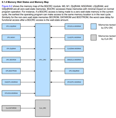
How should we understand the division of non-zero wait registers and zero wait registers mentioned in the BGCRC module? Are all ROM non-zero wait and RAM zero wait? Or is it based on timing?
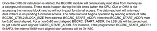
Why is the address aligned with 0x80?
Someone mentioned that BGCRC does not support access to Flash. Is it because Flash is too slow, so BGCRC is not used for checking?
--
Thanks & Regards
