This thread has been locked.

If you have a related question, please click the "Ask a related question" button in the top right corner. The newly created question will be automatically linked to this question.

TMS320F28379D: C2000 memory map questions

Part Number: TMS320F28379D
Other Parts Discussed in Thread: C2000WARE

hello there,

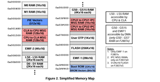
I have a question regrading the memory map of TMS320F28379D \


1) why there is separate block M0,M1 and D0,D1 which have same role but different name ?

2)what are sections in the memory map which available to the user ? 

3) in the below given image why they have used different colors and what is its significance ?

https://www.ti.com/lit/an/sprt720/sprt720.pdf?ts=1708136338055&ref_url=https%253A%252F%252Fwww.ti.com%252Ftool%252FLAUNCHXL-F28379D%253Futm_source%253Dgoogle%2526utm_medium%253Dcpc%2526utm_campaign%253Depd-c2x-null-44700045336317722_prodfolderdynamic-cpc-pf-google-soas_int%2526utm_content%253Dprodfolddynamic%2526ds_k%253DDYNAMIC%2BSEARCH%2BADS%2526DCM%253Dyes%2526gad_source%253D1%2526gclid%253DCjwKCAiArLyuBhA7EiwA-qo80DPpJAZAGJV_WywgvpynQTbbVOmSb3m0DCTiZphUslADBzDKs-6BXxoCjooQAvD_BwE%2526gclsrc%253Daw.ds

  • Hello,

    Due to US holiday, please expect a response by 20th February.

    Thanks & Regards,

    Sinchita

  • Hello Vishanth,

    1) why there is separate block M0,M1 and D0,D1 which have same role but different name ?

    M0 and M1 are smaller and usually used to store items like global variables, jump tables, stack, and constructors (although they can be used for alternative purposes). If you compare a linker command (.cmd) file from an example in C2000Ware with the Linker Command File Primer page, you can see these typical use cases. The reason for this is architecturally how the device is constructed, the M0/1 RAMs are not identical to the Dx RAMs which are more for storing program instructions or data.

    2)what are sections in the memory map which available to the user ? 

    All LSx, GSx, Dx, and Mx RAMs are available. There are recommendations for how to use these memories optimally, but they can be used by the user for whatever purpose they need. The MSGRAMs are dedicated for communication between processors, and as such should not be used for other purposes.

    3) in the below given image why they have used different colors and what is its significance ?

    I'm not overly familiar with this particular document, but based on what I can see it looks like all the gray blocks are "normal" memory (not particularly specialized, besides OTP), red is message RAMs (i.e. CPU to CLA or CPU to CPU), dark blue is the interrupt (PIE) vectors, and light blue is memory relating to boot ROM.