This thread has been locked.

If you have a related question, please click the "Ask a related question" button in the top right corner. The newly created question will be automatically linked to this question.

TMS320F28384D: Accessing EMIF 32bit Address

Part Number: TMS320F28384D

Dear Sir ,

We are developing Controller  based on C2000 28384D  , And  Accessing   FPGA  Registers and Memory  using  EMIF interface  in ASRM mode  32bit Data width configuration.   

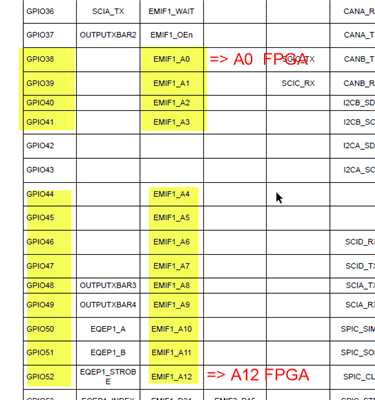
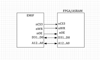
for  the addresses  we have connected   A0...A12    , and Data  D31..D0.

the Access  is done  via CS3   (e.g.     Address range starting at  0x300000 ....).

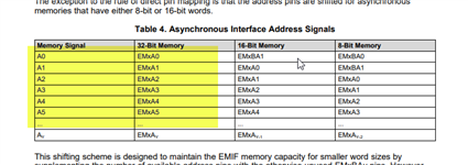
we are seeing  some  shift in the address  ,  that is unclear to us    . if we have  access  of 32bit  only (using DMA/CPU )  we expected  that the access  to the next address  will be +1

(we  are probing  the Address bus  from A0...A12 )

e.g.  

*(long *)0x300000=0;    // A0...A12   all 0 

*(long *)0x300001=1;   //A0 =1  , A1..A12  all 0

*(long *)0x300002=2;   //A0 =0  , A1 =1  , A2..A12=0

...

but  the above  is not  true  (this was tested with DMA in 32bit mode , and using CPU)  , we are seeing some shift  as shown below , it looks like  that in order to access  to the next address  we need to add  +2

*(long *)0x300000=0;    // A0...A12   all 0 

*(long *)0x300002=1;   //A0 =1  , A1..A12  all 0

*(long *)0x300004=2;   //A0 =0  , A1 =1  , A2..A12=0

this is  how it is supposed  to work ?  i assumed  that if  i am accessing the FPGA  as 4Kx32bit  memory  each  address  will be separated by +1 

  • Hello Eyal,

    but  the above  is not  true  (this was tested with DMA in 32bit mode , and using CPU)  , we are seeing some shit  as shown below , it looks like  that in order to access  to the next address  we need to add  +2

    To clarify, is the address values listed the EMIF address values on the GPIO pins or are you looking at the access by the DMA to the value in memory? If it's the latter, can you explain your DMA configuration or show how your setting it up to access the memory via EMIF?

  • Hi Omer  ,

    I am probing the Actual  GPIO  (A0,A1,.....)  and CS

  • Hi Eyal,

    Okay, so the DMA is accessing the EMIF and using the addresses shown above which are incrementing by 2. This doesn't seem like something caused by the EMIF, but the DMA. Can you show me your DMA setup? It's possible it could be trying to access more words than you intend, which could be why the address pins are incrementing by 2.

    Also, you could verify whether this is the case by disabling the DMA and trying to just access the EMIF addresses one at a time. If this works as expected, than likely the source of the discrepancy is from the DMA configuration.

  • I have  tried  both  scnerio 

    Direct Access     (in order  to force  32bit address i even  used     __byte_peripheral_32((volatile unsigned long *)0x300200)=my32;   , this  will make sure  that the access is indeed 32bit , but it is resulting the same  , only increment of +2  cause  the address  to change 

    i mean accessing     0x300200  and  0x300201  will result  the same  .

    with DMA   , same issue   (Data size  = 32bit  )     only  setting  DST STEP  =2    will cause  to write  to different address  (DST STEP =1  , is not correct)

    i saw  in the reference   the following  which explains  the DMA  , i am guessing  it is the same  for direct access


  • i mean accessing     0x300200  and  0x300201  will result  the same  .

    Sorry, I realize this might sound trivial but can you double-check that your accessing the correct GPIO pins for your EMIF address bits? If accessing an odd address is not appearing on the address pins, then this might be one cause. You could also verify this by trying to access each address from 0x1 to 0x800 by just shifting the bit left (i.e. 0x1, 0x2, 0x4, 0x8...0x800) to see if any bits besides A0 are behaving strangely. In the meantime, I will check with another expert regarding whether this behavior is expected for using EMIF in 32-bit mode.

  • Can you also provide a connection diagram between the EMIF and the external device? Something akin to the below image (although the right device for your case would be a 32-bit ASRAM):

  • below   are  the pins  for A0...A12    as i am accessing  32bit  only  i don't  use  BA0 and BA1

    Odd and even  give the save  result   e.g.     0x300200  and  0x300201   (so one  0x300202  and 0x300203)

  • the scheme connection between the C2000 EMIF  to FPGA/ASRAM  as  mention above  , i follow  the EMIF guide lines  as described below 


  • Hello Eyal,

    below   are  the pins  for A0...A12    as i am accessing  32bit  only  i don't  use  BA0 and BA1

    Odd and even  give the save  result   e.g.     0x300200  and  0x300201   (so one  0x300202  and 0x300203)

    Sorry, your response isn't clear to me. Did you try accessing the addresses 0x1, 0x2, 0x4, 0x8...0x800 to make sure each address pin A# gets toggled? I know that A0 doesn't seem to produce a difference, what I'm trying to determine is whether you have the correct connections set up. If accessing 0x0 and 0x1 outputs 0x0 on the address lines, that makes me believe that the address lines are not connected properly. Since I can't see your hardware setup, this is why I asked you to read the pins for these addresses.

    You showed a table from the reference manual regarding the GPIO connections, which is correct, but please try to access addresses to make sure each corresponding address pin gets toggled. Especially for GPIO41 and GPIO52, as possible misalignment of your address pins should show up on one of these two pins.

  • i can  cause   any  of the address bit to  toggle  by   accessing    1<<(Ai+1)  , e.g  to toggle A0     1<<(0+1)   =2    , toggle A1   1<<(1+1)=4    ,                    toggle  A2 1<<(2+1) =8 , etc  toggle  Ai   1<<(i+1)

    i can  access  the whole address space  in the ASRAM  , the writes and read are valid  ... it is  just seen that when the DSP is accessing  it requries  +2  

    all connection were double checked 

  • Hello Eyal,

    Can you share your EMIF configuration code? I will take a look at it and see if I can find an explanation for this with another expert.

  • Hi Eyal,

    I spoke with some other experts, and based on their explanation it would make sense that 0x300200 and 0x300201 would access the same address; the reasoning being that even though the external memory may be 32-bits, the C28 memory is only 16-bits so there would need to be two separate reads to read the upper and lower half of the 32-bit data. I apologize for any confusion I may have caused earlier with my posts, I will let you know if I learn anything else but for now this seems to be expected behavior based on the memory width of our devices.