This thread has been locked.

If you have a related question, please click the "Ask a related question" button in the top right corner. The newly created question will be automatically linked to this question.

TMS320F280039C: AD sampling instability issue

Part Number: TMS320F280039C

Hi Team,

Customers encountered the problem of unstable AD module sampling when using F280039. The phenomenon is that the external signal sent to the AD port is stable and clean, but after the AD-converted signal inside the MCU is printed out through the DAC, it is found that there is a lot of interference on the signal, as shown in the figure below. The input signal of the ADC is a 0-3.3V sampling signal.

Yellow and green are the values in the internal ADC module result register output by the DAC, it looks like there is a problem with the AD module working.

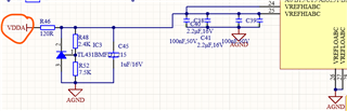
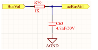
The following is the customer's configuration of the ADC module, using external power supply.

--

Thanks & Regards

  • Hello Yale,

    What do the ADC input network and voltage reference circuits look like?

    Thanks,
    Ibukun

  • Hello Ibukun,

    As shown in Figure 1 below, the customer's voltage reference circuit, VDDA is 5V, and 3.3V is generated through the voltage regulator device to power the ADC external reference.
    In the experiment, the voltage waveforms of Pin24 and Pin25 were tested, and 3.3V was stable.

    Figure 1

    Figure 2 below shows the customer's sampling network. Bus+ and Bus- are high voltages of about 800V. They are sent to the ADC port (ucBusVol) after voltage division and differential circuit conditioning. The measured signal is also stable.

    Figure 2

    In addition, they would like to ask whether the problem is related to the MCU layout? They now separate the analog and digital grounds in the layout.

    --

    Thanks & Regards

  • Thanks Yale.

    One other quick question -- is the customer by any chance using DMA to transfer ADC results? If so, are they properly accounting for the errata advisory "ADC: DMA read of stale result"?

    Thanks,
    Ibukun

  • Hello Ibukun,

    They are not using DMA to transfer ADC results. ADC triggered by ePWM SOC. After conversion complete, ADCINT is triggered, then read ADC results in ADC ISR.

    --

    Thanks & Regards

  • Hi Yale,

    Please see my comments below.

    As shown in Figure 1 below, the customer's voltage reference circuit, VDDA is 5V, and 3.3V is generated through the voltage regulato

    Is VDDA supply and VDDIO supply generated from the same regulator?  When these supplies are ganged, switching noise from the digital logic may couple to the VREF line.  This could be a potential reason for the noise being observed.

    Figure 1 (input network) shows a string of 6 470k resistors (~2.8M series resistance per input).  I do not see any voltage divider though so it seems to be that the 800V goes directly to the ADC channels, which obviously is not correct.  Maybe there is a missing resistor going to ground that is not shown in the diagram?

    Regardless, the input network involves the use of high value resistors and capacitance that directly connects to the ADC inputs and this would require higher ACQPS because of this impedance for the ADC to properly sample the signal.  Can you check what ACQPS value that the customer is using?

    Thanks,

    Joseph

  • Hi Joseph,

    Is VDDA supply and VDDIO supply generated from the same regulator?  When these supplies are ganged, switching noise from the digital logic may couple to the VREF line.  This could be a potential reason for the noise being observed.

    The figure below shows the complete power supply network of the customer's MCU. The MCU digital power supply VDDIO and analog power supply VDDA are generated by the same LDO, but the two are connected through magnetic beads. The external power supply for the ADC module is generated by another LDO. Is there any problem with supplying VDDA and VDDIO like this? Their previous project plans used an LDO to generate two power supplies, and the actual power supply signals were stable.

    Figure 1 (input network) shows a string of 6 470k resistors (~2.8M series resistance per input).  I do not see any voltage divider though so it seems to be that the 800V goes directly to the ADC channels, which obviously is not correct.  Maybe there is a missing resistor going to ground that is not shown in the diagram?

    Sorry for the problem with the previous statement. Bus+ and Bus- directly enter the differential amplifier circuit without voltage division.

    Regardless, the input network involves the use of high value resistors and capacitance that directly connects to the ADC inputs and this would require higher ACQPS because of this impedance for the ADC to properly sample the signal.  Can you check what ACQPS value that the customer is using?

    The following figure shows the customer's ACQPS configuration. ACQPS = 10. All sampling channels are configured the same. Is there any problem with this configuration?

    --

    Thanks & Regards

  • Hi Yale,

    What is not clear to me is how BUS VO+ and BUS VO- connects to the ADC input of the F280039.  Does it connect directly to BusVol node with the the 1K/4.7nF input network?

    I see that ACQPS uses the minimum value but with the RC impedances involved, acqps should be way higher.  Please see section 16.13.2 Choosing an Acquisition Window Duration of the TRM on how ACQPS is derived.  This would also impact accuracy of conversion.

    Regards,

    Joseph 

  • Hi Joseph,

    The customer re-described their voltage sampling circuit: the two resistors R109 and R131 in the picture are not actually used. They are actually a simple differential amplification followed by two stages of RC filtering and sent to the MCU port. The voltage calculation formula after conditioning is: 

    ucBusVol = R105/Sum(R98+R99+R100+R101+R102+R103+R106) * (Bus+ - Bus-)

    In addition, the customer read the description of ACQPS calculation in section 16.13.2 and has a question to ask.
    Do Rs and Cs in the figure below correspond to the last stage RC filter parameters in their circuits? That is, the parameters shown on the right.
    If so, they plug it into the formula to calculate, and the corresponding ACQPS should be 13. Currently, they set it to 10. It doesn't seem to be much different than what you said. Later they will change the ACQPS value to verify whether this is the problem. But they usually put multi-stage RC filtering in the sampling circuit. At this time, do Rs and Cs only consider the parameters of the level close to the MCU port?

    --

    Thanks & Regards

  • Yale,

    It represents the equivalent RC of the entire input network, not just the components that are close to the pin. Assuming you treat the op amp as ideal with zero output impedance, the computation is on everything else after it.

    Best regards,

    Ibukun