


Part Number: LAUNCHXL-F2800137
Other Parts Discussed in Thread: TIDM-DC-DC-BUCK, TIDM-02000, POWERSUITE, SFRA
Hi,
I implemented a peak current mode control with slope compensation following the documents listed below:
- Step-by-Step Design Guide for Digital Peak Current Mode Control: A Single-Chip Solution (Biricha Digital Power LTD)
- SPRABE7A: Digital Peak Current Mode Control With Slope Compensation Using the TMS320F2803x.
But I have some doubts.
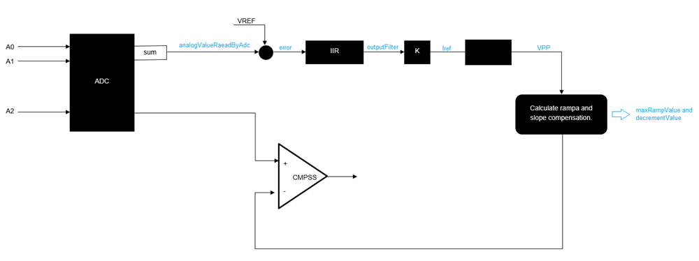
I have an ePWM with Fswitching = 100KHz and every 100KHz the ADC interrupt occurs to read the analog inputs and perform the calculation of maxRampValue and decrementValue. In particular:
1) I calculate the error as: error = VREF - analogValueReadByAdc. Where VREF is calculated as reported in the Biricha document with the Equation 19: ![]() where ADCbits = 12 and VDAC = 3,3V.
where ADCbits = 12 and VDAC = 3,3V.
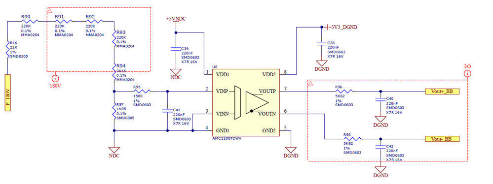
The image below, shown our feedback signal where RB = 884k21 and R1 = 1k05; in to out gain of the IC in differential mode is x8. How do we insert this value in VREF calculation?
2) The error is the input for a 2p2z filter that give me an output called outputFilter.
3) I multiplied the outputFilter for K calculated as reported in the SPRABE7A (pag 3 equation (1) ) ![]() where
where
- SamplingGain = 1.71
- ADCmaxV = 3.3V
- ADCbits = 12
- DACbits = 12
- DACmaxV = 3,3V
I called Iref = K * outputFilter
4) I calculate VPP as reported in the SPRABE7A (pag 7, equation (20)) ![]() where D = is the duty cycle of the ePWM read by the eCAP, Ri = 200mOhm, Ts = 10us, Vin = Iref, L0 = 200uH.
where D = is the duty cycle of the ePWM read by the eCAP, Ri = 200mOhm, Ts = 10us, Vin = Iref, L0 = 200uH.
Ri = 200mOhm is the equivalent of the transformation factor of the current sensor CT425-HSN820MR (200mV/A) that we are using.
5) I calculate the maxRampValue and the decrementValue for the ramp configuration with the equations reported below:
-
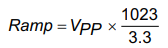 is the equation used in SPRABE71 where 1023 is the DAC bits and 3.3 is the DACmax V. This equation is the same of the Biricha document without the factor 64:
 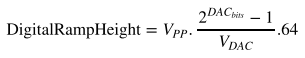 In fact, in my calculation I set ramp value with this formula: Ramp = VPP * (4095/3.3) because my DAC is 12 bits and DAC range is 3.3V.
 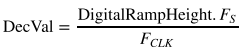 is the equation used in Biricha document and in my application Fs = 100KHz and Fclk = 100MHz.
Are the steps reported above correct? Are the formulas correct? Do I need to perform other calculations for peak current mode control?
I attached a schematic of my control.
Is there a way to monitor the ramp waveform? If I wont ramp value in volt, how can I do?
Thank you in advance.
Best Regards,
Debora
