This thread has been locked.

If you have a related question, please click the "Ask a related question" button in the top right corner. The newly created question will be automatically linked to this question.

TMS320F280039: Why VDAC/B3 floating only infect CMPSS3 function?

Part Number: TMS320F280039

Hi Team, 

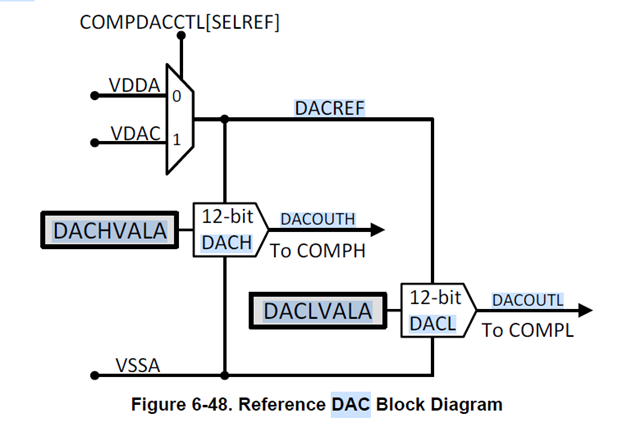
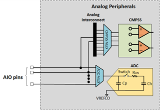
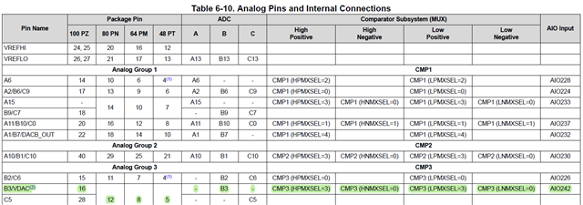
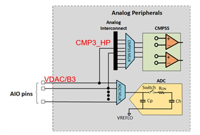
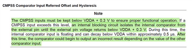
The CMPSS reference voltage is configured to use VDDA and VDAC is not enabled. When the VDAC/B3 pin is in a floating state, why does it interfere with the CMPSS3 comparator and cause the comparator result to be incorrect?

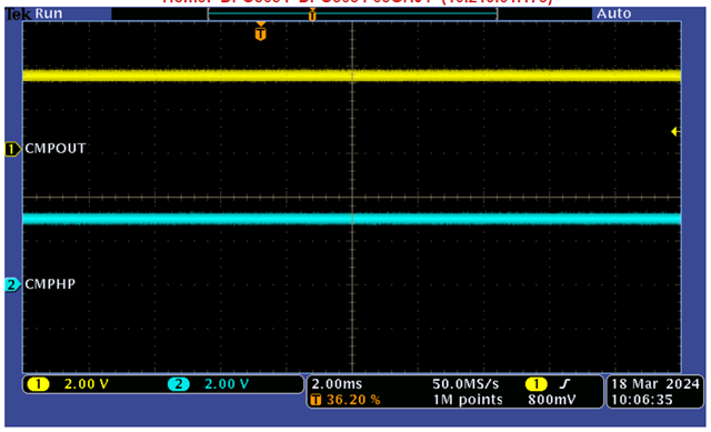
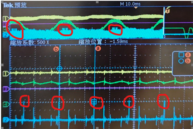
The CMPSS signal is far from reaching the set threshold, but the protection is triggered in advance (the threshold is set to trigger at 2.9V, but the actual input signal is only 2.1V).

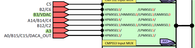
CMPSS1/3/4 are used at the same time, but only CMPSS3 triggers protection in advance, and the other two trigger normally without problems. The input signal of CMPSS3 is the A3 pin.

Best Regards,

Zane

  • Hi Zane,

    Thanks for your patience.

    I have some questions:

    1) The threshold is coming from pin or internal DAC? if it is coming from pin, are you using ADC to read the value of the signal on the pin?

    2) what is the reference voltage? 1.65V or 2.5V?

    Regards,

    Hadi

  • Hi Hadi,

     CMPSS3 reference voltage is configured to use VDDA. But when let VDAC/B3 floating, it will infect A3. 

    Could you give me some explain? Here is the same problem:(+) TMS320F280049: EPWM giving nuisance trip on ADC pin B3,VDAC - C2000 microcontrollers forum - C2000Tm︎ microcontrollers - TI E2E support forums

    Best Regards,

    Zane

  • Zane,

    The only difference between VDAC/B3 pin and other pins is VDAC/B3 has a higher capacitance. 

    I will try this test in my side to see how it works. In the meantime, can you use a pull-down resistor on VDAC/B3 and see how it works?

    Regards,

    Hadi

  • Hi Hadi,

    The customer has let VDAC/B3 to GROUND. Now it can work. But customer want to why this happen?

    Best Regards,

    Zane

  • Zane,

    Thanks for confirming that.

    The voltage on a floating pin is undetermined and mostly based on the parasitic RC network on the pin. The VDAC/B3 pin has a higher capacitance than the other analog pins and hence any voltage will take longer to bleed off depending on the RC network formed on the pin.

    Regards,

    Hadi

  • Hi Hadi, 

    Thanks for your patience! Did you test that when VDDA is used as the reference voltage, and VDAC float causes an exception for CMPSS3, but not CMPSS1 and CMPSS4. The customer is in a hurry to know why this is happening and would like us to give a reasonable explanation. 

    Best Regards,

    Zane

  • Hi Hadi, 

    Are there have any update, customer is very urgent to know the root of the problem. I will very grateful if you do some test and give us some reasonable reason. Thanks a lot!

    Best Regards,

    Zane

  • Hi Zane,

    I tried to reproduce the issue in my end, but CMPSS3 is working fine. 

    Here you can see the results of a test with B3/VDAC floating while I give 2.91V to A3 and internal DACH is using VDDA and set to 3600. As you can see the output goes to High.

    When a signal of 2.88V is applied, the output goes to Low:

    is customer using any RC filter for pin A3? please share more info about their circuit's signal conditioning. 

    Regards,

    Hadi

  • Hi Hadi,

    Thanks for your confirm! There are many noises on customer's board. 


    CMPSS3 early triggering problem, false haptations are not continuous triggering, but are pulsed. In general, continuous triggering is true to the threshold; the pulse form, which may be due to factors such as interference, causes the comparator results to be incorrect.

    As shown below, the trigger is at the red circle. False haptations occur at the peak of the input current and when the mos tube is switched.
    So our own judgment is that the mos tube is switching state interfering with the B3/VDAC, which in turn interferes with the reference voltage of CMPSS3 (for example, assuming the reference voltage of 3.3V set by the CMPSS, Interference causes the actual reference voltage to be 2.3 volts, leading to an early trigger protection).
    CH2: CMPOUT
    CH4: Input current for current gun test

    Do we have an internal architecture diagram of the comparator module?
    Whether it is possible that interference is affecting other pins on the CPMSS3 MUX, causing the pin voltage to exceed 3.3V.  The VDAC/B3 pin to be grounded will effectively resolve this issue.

    Best Regards,

    Zane

  • Hi Hadi,

    Please see below, it not only occur on F280039, but also occur on F280049.

    Please help us to find out! Thanks a lot!

    TMS320F280049: EPWM giving nuisance trip on ADC pin B3,VDAC - C2000 microcontrollers forum - C2000Tm︎ microcontrollers - TI E2E support forums

    Best Regards,

    Zane

  • Hi Zane,

    Here you can find the simplified schematic of the analog peripheral interconnection. the more detailed analog subsystem diagram is shown in Figure 12.1 in TRM

    Also, the reference DAC of CMPSS module is shown in Figure 16.3. As you can see, the comparator reference is coming from either VDDA or VDAC and can be selected using register COMPDACCTL[SELREF]. So, in your case, the VDDA is used.  However, from the result you provided it is clear that due to the crosstalk, the noise from switching activity in the circuit is coupled to the input pin of comparator and false trigger is happening. 

    Here are some quick design tips for suppressing crosstalk:

    1) Reduce the length that two lines are allowed to run in parallel. A minimum spacing of three times the signal width is a good rule of thumb. Be sure to have solid return paths where possible. Reducing the separation between signal and ground ensures the signal has a good return path. A TI article that gives more details on different considerations and PCB layout tips to reduce crosstalk an be found here. The article has applicable information to help reduce the crosstalk issue you are experiencing. 

    2) The Low-Pass Filter mode is the best to use for repetitive sampling applications where momentary glitches or high-frequency noise is present in the signal.

    Regards,

    Hadi

  • Zane,

    In the thread you're mentioning here, the customer was reading B3/VDAC pin in his ADC interrupt, which isn't the case for your customer. You're not reading B3/VDAC pin. 

    In between the analog MUX and the ADC is a sample and hold circuit. So each time you switch the MUX from on signal to another, then you couple the old level to the new signal. The time required to charge is dependent on the driver impedance.

    Here are my questions:

    1) What values of RC is customer using for A3 pin?

    2)what channels are used for ADC readings?

    3) ask customer to enable internal pull-ups on pin B3/VDAC and let me know how the comparator behaves. By default, this pin functions as analog pins and the GPIOs are in a high-impedance state. The GPyAMSEL register is used to configure these pins for digital or analog operation. They need to use following function to enable pull-up internally on AIO242: 

    GPIO_setPadConfig(242, GPIO_PIN_TYPE_STD | GPIO_PIN_TYPE_PULLUP);

    Regards,

    Hadi

  • Hi Hadi,

    Thanks for your help.

    In fact, my customer use VDAC/B3 as ADC input, in this situation, the result is better than VDAC/B3 floating, but still have the pre-trigger problem.

    I will confirm the two questions you asked with the customer tomorrow morning.

    Best Regards,

    Zane

  • Hi Hadi,

    The follwing is a schematic of VDAC/B3 and CMP3_input pin, which are actually connected together before the internal MUX. Whether my understanding is correct? If my understanding is correct, it also explains why the VDAC/B3 state only affect CMP3, but not CMP1&CMP4.

  • Zane, 

    If customer is reading VDAC/B3 using ADC, then they shouldn't leave that pin floating as there is a sample and hold circuit in the ADC. So each time you switch the MUX from on signal to another, then you couple the old level to the new signal. The time required to charge is dependent on the driver impedance. Leaving pin VDAC/B3 float means a high impedance which doesn't discharge the voltage on sample/hold capacitor. That's why the customer sees a false trigger.

    Regards,

    Hadi

  • Zane,

    Yes that's correct. VDAC/B3 is connected to CMP3_input pin.

    Regards,

    Hadi

  • Hi Hadi,

    Thanks for your help! The problem has been solved. Do not allow the pins to floating. It maybe cause some IO voltage over VDDA+0.3. 

    Best Regards,

    Zane