This thread has been locked.

If you have a related question, please click the "Ask a related question" button in the top right corner. The newly created question will be automatically linked to this question.

TMS320F28027F: Question on measured SPI clock waveform

Part Number: TMS320F28027F


I looked at the analog waveform for the SPI signals on Launchpad, running a TI demo project, but with MOSI connected to MISO on the Launchpad.  Data transmit/receive are correct, so SPI seems to be operating correctly

I this for the clock signal

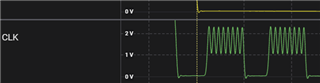
Is this correct that the clock oscillation is in this form?  If yes, is there documentation that describes this?  I didn't see anything in the datasheet that discusses voltage levels for the SPI clock output.

Thanks,

  • Hi Mark,

    The "correct" clock mode for SPI communication depends on the devices that are communicating. As long as both devices (slave and master) are expecting the same clocking scheme (e.g. transmitting data on the rising edge of SPICLK and latching data to receive on the falling edge, which would be phase 0 polarity 0 on a C2000 device according to our device TRM), then communication will happen as expected and be transmitted/read properly at the same time by both devices. 

    So in summary, the master (the device controlling the clock) should use/send out a SPICLK signal that matches what the slave device expects. Typically, other devices will have images of a SPI clocking scheme in their datasheets and you can compare that with the modes listed in the TRM to select the one that matches. For the demo projects with MOSI and MISO connected, this is not an issue because the device is communicating with itself (if I'm understanding correctly that the example projects you are running are loopback examples). The voltage levels would be like any high/low output voltage from the device.

    Let me know if this helps or you have further questions!

    Best Regards,

    Allison