


Part Number: TMS320F28386D
HELLO ,
I am working on new customize pcb board using f28386D MCU
when i am try to flash the programme in flash or ram i am getting error
i am using XDS110 DEBUG PROBE
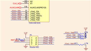
This is the connector schematic of JTAG right now i am using this connection .
NOTE :- iam not using P3->pin3
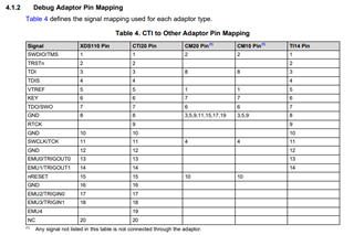
this tis the datasheet of debugger and information based on datsheet i am using 20 pin to 14 pin converter and 14 pin converterto 7 pin .
Please confirm is this JTAG connection schematic is correct or not .
while dumping code i am getting below error
C28xx_CPU1: Flash Programmer: Unable to acquire the pump semaphore. The other core might still be accessing the pump registers. Operation Cancelled.
C28xx_CPU1: File Loader: Memory write failed: Unknown error
C28xx_CPU1: GEL: File: C:\Users\kumar\workspace_v12\adc\CPU1_FLASH\adc.out: Load failed.
AND this error also
28xx_CPU1: Error occurred during flash operation: Timed out waiting for target to halt while executing init.alg
C28xx_CPU1: Error during initialization (Flash algorithm timed out). Operation cancelled.
C28xx_CPU1: Perform a debugger reset and execute the Boot-ROM code (click on the RESUME button in CCS debug window) before erasing/loading the Flash. If that does not help to perform a successful Flash erase/load, check the Reset cause (RESC) register, NMI shadow flag (NMISHDFLG) register and the Boot-ROM status register for further debug.
C28xx_CPU1: File Loader: Memory write failed: Unknown error
C28xx_CPU1: GEL: File: C:\Users\kumar\workspace_v12\led_ex1_blinky\CPU1_FLASH\led_ex1_blinky.out: Load failed.
i am using example code led blinky.
Kindly Let me know how to Debug the HARDWARE


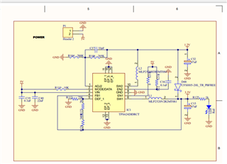 this my power supply is correct or not