Other Parts Discussed in Thread: ADS8326, C2000WARE, CONTROLSUITE
Hello,
I am a beginner with the F28027 and am trying to configure SCI. I have succeeded in configuring the device for 9600 Baud, but am having trouble increasing it to 115200.
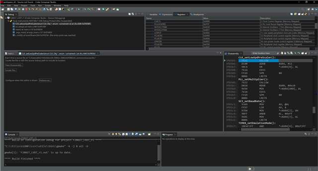
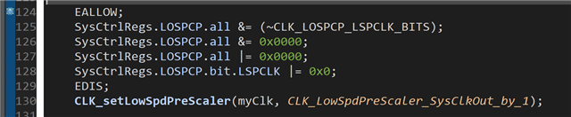
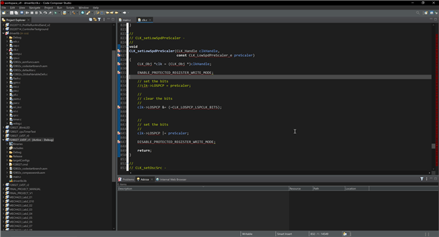
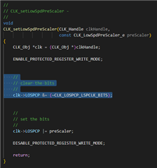
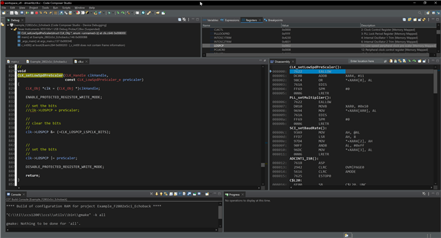
First, I set the low speed clock prescaler (LOSPCP) to /1.
CLK_setLowSpdPreScaler(myClk, CLK_LowSpdPreScaler_SysClkOut_by_1);
Next, I set the BRR register value, which I calculated as follows:
BRR = (60MHz/(115200*8))-1 = 64.10 ~ 64
Back calculate Baud --> (60MHz)/((16+1)*8) = 115384.61 Baud, 0.16% error
SCI_setBaudRate(mySci, (SCI_BaudRate_e)64);
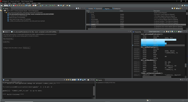
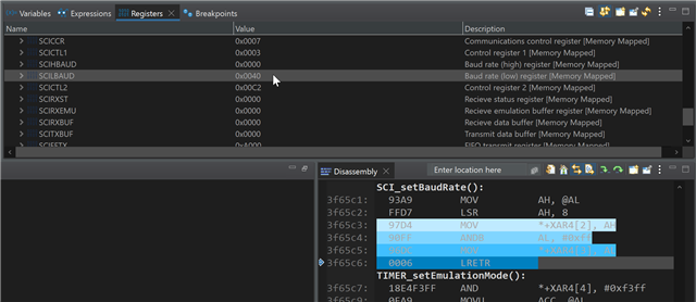
When I open the Terminal, the transmission is a bunch of random characters.
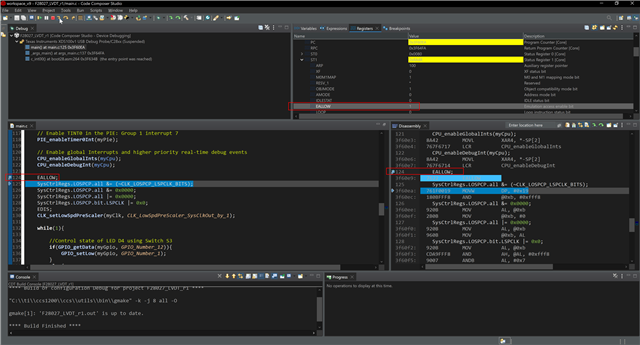
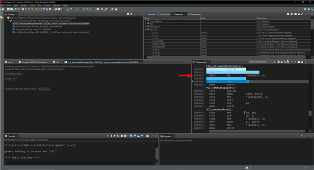
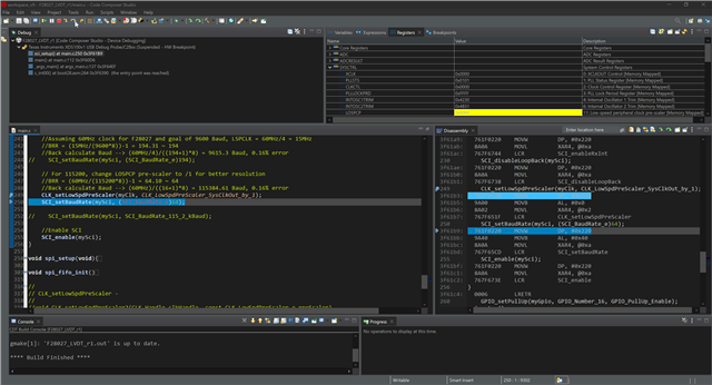
I double checked the registers and found that BRR is updating as expected, but LOSPCP is not changing from the default 0x0002. 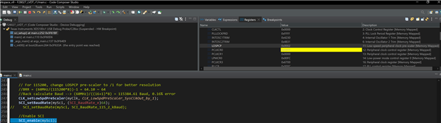
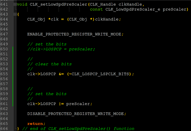
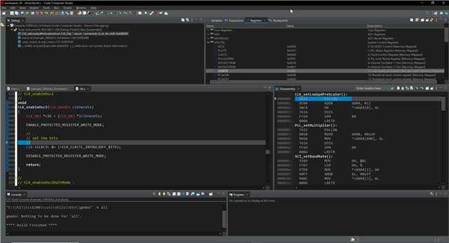
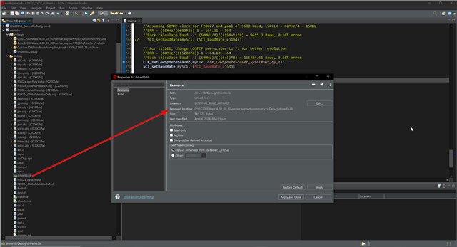
I am using the CLK_setLowSpdPreScaler() function but it doesn't seem to have an effect. I looked at the clk.c file and it seems to handle EALLOW and EDIS, so I'm assuming that's not the problem.
Does something else need to be changed or set in order to modify LOSPCP? I'm sorry if this is a basic question but I'm struggling to find information in the reference manual about changing this register besides needing to set EALLOW.
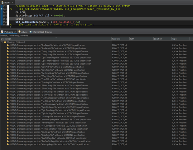
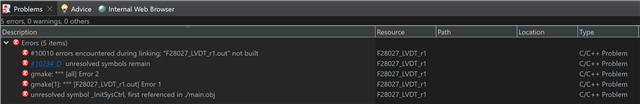
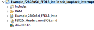
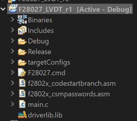
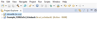
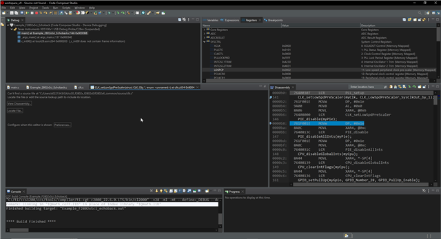
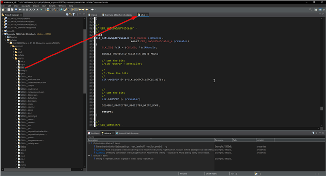
Here is a screenshot of the project:
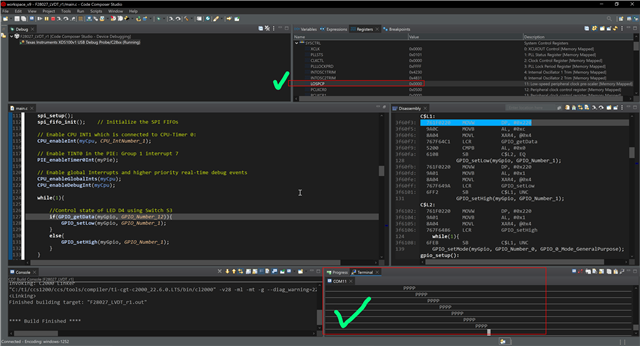
Here is my main.c :
#include "DSP28x_Project.h" // Device Headerfile and Examples Include File (includes stdint.h)
// Include driver header files#include "f2802x_common/include/adc.h"#include "f2802x_common/include/clk.h"#include "f2802x_common/include/gpio.h"#include "f2802x_common/include/pie.h"#include "f2802x_common/include/pll.h"#include "f2802x_common/include/timer.h"#include "f2802x_common/include/wdog.h"#include "f2802x_common/include/sci.h"#include "f2802x_common/include/spi.h"
// Declare function prototype__interrupt void cpu_timer0_isr(void);void gpio_setup(void);void sci_setup(void);void spi_setup(void);void spi_fifo_init(void);
// Declare HandlesADC_Handle myAdc;CLK_Handle myClk;GPIO_Handle myGpio;PIE_Handle myPie;TIMER_Handle myTimer;SCI_Handle mySci;SPI_Handle mySpi;
int main(void){ // Declare local handles CPU_Handle myCpu; WDOG_Handle myWDog; PLL_Handle myPll;
// Initialize handles myAdc = ADC_init((void *)ADC_BASE_ADDR, sizeof(ADC_Obj)); myClk = CLK_init((void *)CLK_BASE_ADDR, sizeof(CLK_Obj)); myCpu = CPU_init((void *)NULL, sizeof(CPU_Obj)); myGpio = GPIO_init((void *)GPIO_BASE_ADDR, sizeof(GPIO_Obj)); myPie = PIE_init((void *)PIE_BASE_ADDR, sizeof(PIE_Obj)); myPll = PLL_init((void *)PLL_BASE_ADDR, sizeof(PLL_Obj)); myTimer = TIMER_init((void *)TIMER0_BASE_ADDR, sizeof(TIMER_Obj)); myWDog = WDOG_init((void *)WDOG_BASE_ADDR, sizeof(WDOG_Obj)); mySci = SCI_init((void *)SCIA_BASE_ADDR,sizeof(SCI_Obj)); mySpi = SPI_init((void *)SPIA_BASE_ADDR, sizeof(SPI_Obj));
// Initialize watchdog handle and disable. myWDog = WDOG_init((void *)WDOG_BASE_ADDR, sizeof(WDOG_Obj)); WDOG_disable(myWDog);
// Load oscillator calibration values using Device_cal // According to TRM section 1.3.2.1.2, ADC clocks must be enabled to calibrate the oscillators and ADC parameters. CLK_enableAdcClock(myClk); (*Device_cal)(); CLK_disableAdcClock(myClk); //Since the ADC is not needed for this application, it is disabled once calibration is done.
// Set internal oscillator 1 as the clock source. CLK_setOscSrc(myClk, CLK_OscSrc_Internal);
// Internal oscillator 1 runs at 10MHz, I need 60MHz. Multiply 10MHz by 12, divide by 2 PLL_setup(myPll, PLL_Multiplier_12, PLL_DivideSelect_ClkIn_by_2);
//Disable PIE and all interrupts before changing PIE PIE_disable(myPie); PIE_disableAllInts(myPie); CPU_disableGlobalInts(myCpu); CPU_clearIntFlags(myCpu);
// Re-enable PIE PIE_enable(myPie);
// Register interrupt handlers in the PIE vector table // Group number and subgroup number from TRM Table 1-110. PIE_registerPieIntHandler(myPie, PIE_GroupNumber_1, PIE_SubGroupNumber_7, (intVec_t)&cpu_timer0_isr);
#ifdef _FLASH memcpy(&RamfuncsRunStart, &RamfuncsLoadStart, (size_t)&RamfuncsLoadSize);#endif
// Configure CPU-Timer 0 to interrupt every 100 milliseconds: // 60MHz CPU Frequency TIMER_stop(myTimer); TIMER_setPeriod(myTimer, (uint32_t)(60 * 100000)); TIMER_setPreScaler(myTimer, 0); TIMER_reload(myTimer); TIMER_setEmulationMode(myTimer, TIMER_EmulationMode_StopAfterNextDecrement); //Note this is the default. TIMER_enableInt(myTimer);
TIMER_start(myTimer);
//Initialize GPIO gpio_setup();
//Set up SCIA sci_setup();
//Set up SPI spi_setup(); spi_fifo_init(); // Initialize the SPI FIFOs
// Enable CPU INT1 which is connected to CPU-Timer 0: CPU_enableInt(myCpu, CPU_IntNumber_1);
// Enable TINT0 in the PIE: Group 1 interrupt 7 PIE_enableTimer0Int(myPie);
// Enable global Interrupts and higher priority real-time debug events CPU_enableGlobalInts(myCpu); CPU_enableDebugInt(myCpu);
while(1){
//Control state of LED D4 using Switch S3 if(GPIO_getData(myGpio, GPIO_Number_12)){ GPIO_setLow(myGpio, GPIO_Number_1); } else{ GPIO_setHigh(myGpio, GPIO_Number_1); } }
}
void gpio_setup(void){ //LED D2 is connected to GPIO0. Set GPIO0 to GPIO configuration, output direction, and disable pull-up. GPIO_setMode(myGpio, GPIO_Number_0, GPIO_0_Mode_GeneralPurpose); GPIO_setDirection(myGpio, GPIO_Number_0, GPIO_Direction_Output); GPIO_setPullUp(myGpio, GPIO_Number_0, GPIO_PullUp_Disable); GPIO_setHigh(myGpio, GPIO_Number_0); //Initialize GPIO0 to known state
//LED D4 is connected to GPIO1. Set GPIO1 to GPIO configuration, output direction, and disable pull-up. GPIO_setMode(myGpio, GPIO_Number_1, GPIO_0_Mode_GeneralPurpose); GPIO_setDirection(myGpio, GPIO_Number_1, GPIO_Direction_Output); GPIO_setPullUp(myGpio, GPIO_Number_1, GPIO_PullUp_Disable); GPIO_setHigh(myGpio, GPIO_Number_1); //Initialize GPIO0 to known state
//LED D3 is connected to GPIO2. GPIO_setMode(myGpio, GPIO_Number_2, GPIO_0_Mode_GeneralPurpose); GPIO_setDirection(myGpio, GPIO_Number_2, GPIO_Direction_Output); GPIO_setPullUp(myGpio, GPIO_Number_2, GPIO_PullUp_Disable); GPIO_setHigh(myGpio, GPIO_Number_2); //Initialize GPIO0 to known state
//Switch S3 is connected to GPIO12. Set GPIO12 to GPIO configuration, input direction, and disable pull-up. GPIO_setMode(myGpio, GPIO_Number_12, GPIO_0_Mode_GeneralPurpose); GPIO_setDirection(myGpio, GPIO_Number_12, GPIO_Direction_Input); GPIO_setPullUp(myGpio, GPIO_Number_12, GPIO_PullUp_Disable);}
__interrupt void cpu_timer0_isr(void){ uint16_t txData16 = 0xFFFF; uint16_t adcData = 0x0000; uint16_t rxData1 = 0x0000; uint16_t rxData2 = 0x0000; //int i = 0;
//Set GPIO0 for debugging/LED GPIO_setHigh(myGpio, GPIO_Number_0);
//SPI Transmit two 16 bit words to TX FIFO SPI_write(mySpi,txData16); SPI_write(mySpi,txData16);
//Wait for 2 words to arrive while(SPI_getRxFifoStatus(mySpi) != SPI_FifoStatus_2_Words) { }
//SPI Read two 16 bit words from RX FIFO rxData1 = SPI_read(mySpi); rxData2 = SPI_read(mySpi);
//Combine rxData; discard first 6 adcData = ((rxData1 << 6) & 0xFFC0) | ((rxData2 >> 10) & 0x003F);
//UART Transmit //Send 16 bit integer as 4 4-bit integers ( //Terminate with line feed "\n" SCI_putDataBlocking(mySci, (uint8_t)(((adcData & 0xF000) >> 12) + 0x41)); SCI_putDataBlocking(mySci, (uint8_t)(((adcData & 0x0F00) >> 8) + 0x41)); SCI_putDataBlocking(mySci, (uint8_t)(((adcData & 0x00F0) >> 4) + 0x41)); SCI_putDataBlocking(mySci, (uint8_t)(((adcData & 0x000F) >> 0) + 0x41)); SCI_putDataBlocking(mySci, 0x0A); //LF
//Acknowledge interrupt so more interrupts from group 1 can be received. PIE_clearInt(myPie, PIE_GroupNumber_1);
//Set GPIO0 GPIO_setLow(myGpio, GPIO_Number_0);}
void sci_setup(void){ //See Example_2802xSci_FFDLB_int.c and TRM section 9.4 for configuration instructions GPIO_setPullUp(myGpio,GPIO_Number_28,GPIO_PullUp_Enable); GPIO_setPullUp(myGpio,GPIO_Number_29,GPIO_PullUp_Disable); GPIO_setQualification(myGpio,GPIO_Number_28,GPIO_Qual_ASync); GPIO_setMode(myGpio,GPIO_Number_28,GPIO_28_Mode_SCIRXDA); GPIO_setMode(myGpio,GPIO_Number_29,GPIO_29_Mode_SCITXDA);
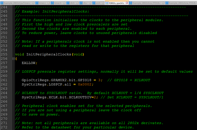
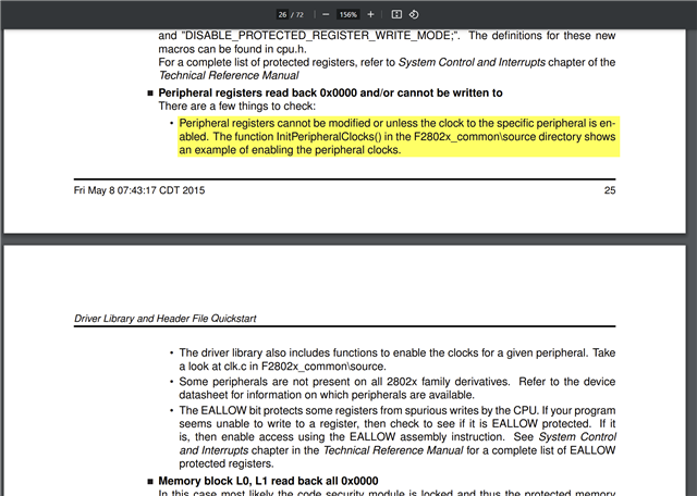
//Peripheral registers cannot be modified unless clock to the specific peripheral is enabled. //Source: Firmware Dev. Package User's Guide, section 2.6. //Enable clock to SCIA CLK_enableSciaClock(myClk);
//Set UART Settings. Parity disabled by default. SCI_disableParity(mySci); SCI_setNumStopBits(mySci, SCI_NumStopBits_One); SCI_setCharLength(mySci, SCI_CharLength_8_Bits);
//Enable Rx, Tx, Rx interrupt, Tx interrupt SCI_enableTx(mySci); SCI_enableRx(mySci); //SCI_enableTxInt(mySci); //Not needed. SCI_enableRxInt(mySci);
//Disable loopback SCI_disableLoopBack(mySci);
//RX ERR, Sleep, and TXWAKE are disabled by default after system reset.
//Set Baud Rate //Clock for SCI comes from LSPCLK, which is just SYSCLKOUT divided down according to LOSPCP register, default /4. //LSPCLK = SYSCLKOUT/(LOSPCP*2) . If LOSPCP = 0, LSPCLK = SYSCLKOUT //Baud rate = LSPCLK / ((BRR+1)*8), or inverse BRR = (LSPCLK/(Baud*8))-1 //BRR is the 16 bit value stored across SCIHBAUD and SCILBAUD // SCI BRR = LSPCLK/(SCI BAUDx8) - 1
//Assuming 60MHz clock for F28027 and goal of 9600 Baud, LSPCLK = 60MHz/4 = 15MHz //BRR = (15MHz/(9600*8))-1 = 194.31 ~ 194 //Back calculate Baud --> (60MHz/4)/((194+1)*8) = 9615.3 Baud, 0.16% error// SCI_setBaudRate(mySci, (SCI_BaudRate_e)194);
// For 115200, change LOSPCP pre-scaler to /1 for better resolution //BRR = (60MHz/(115200*8))-1 = 64.10 ~ 64 //Back calculate Baud --> (60MHz)/((16+1)*8) = 115384.61 Baud, 0.16% error CLK_setLowSpdPreScaler(myClk, CLK_LowSpdPreScaler_SysClkOut_by_1); SCI_setBaudRate(mySci, (SCI_BaudRate_e)64);
//Enable SCI SCI_enable(mySci);}
void spi_setup(void){ // Initialize GPIO for SPI GPIO_setPullUp(myGpio, GPIO_Number_16, GPIO_PullUp_Enable); GPIO_setPullUp(myGpio, GPIO_Number_17, GPIO_PullUp_Enable); GPIO_setPullUp(myGpio, GPIO_Number_18, GPIO_PullUp_Enable); GPIO_setPullUp(myGpio, GPIO_Number_19, GPIO_PullUp_Enable); GPIO_setQualification(myGpio, GPIO_Number_16, GPIO_Qual_ASync); //See TRM 1.4.4.1, SPI peripheral controls synchronization. GPIO_setQualification(myGpio, GPIO_Number_17, GPIO_Qual_ASync); GPIO_setQualification(myGpio, GPIO_Number_18, GPIO_Qual_ASync); GPIO_setQualification(myGpio, GPIO_Number_19, GPIO_Qual_ASync); GPIO_setMode(myGpio, GPIO_Number_16, GPIO_16_Mode_SPISIMOA); GPIO_setMode(myGpio, GPIO_Number_17, GPIO_17_Mode_SPISOMIA); GPIO_setMode(myGpio, GPIO_Number_18, GPIO_18_Mode_SPICLKA); GPIO_setMode(myGpio, GPIO_Number_19, GPIO_19_Mode_SPISTEA_NOT);
// Set GPIO 32 and 33 to inputs because they are jumped by traces to GPIO 16 and 17 //32 and 33 default to GPIO (see GPBMUX1 register), input direction (GPBDIR), enabled pull-up (GPBPUD).
//Enable clock first to allow change of configuration registers. CLK_enableSpiaClock(myClk);
//Set SPISWRESET bit, as directed by TRM 8.4.2 //This will also clear the OVERRUN_FLAG and INT_FLAG bits SPI_reset(mySpi);
// Enable master mode SPI_setMode(mySpi, SPI_Mode_Master); SPI_enableTx(mySpi);
//ADC is TI ADS8326, positive edge for DOUT SPI_setClkPhase(mySpi, SPI_ClkPhase_Normal); SPI_setClkPolarity(mySpi, SPI_ClkPolarity_OutputFallingEdge_InputRisingEdge);
SPI_setBaudRate(mySpi, SPI_BaudRate_1_MBaud); //DIFFERENT VALUE MIGHT BE NEEDED SINCE ENUM ASSUMES 12.5MHz //ADC can handle 24kHz to 6MHz. 15/12 = 1.25MHz
// Set 16-bit char bits SPI_setCharLength(mySpi, SPI_CharLength_16_Bits);
// Release SPI from Reset SPI_enable(mySpi);
return;}
void spi_fifo_init(){ // Initialize SPI FIFO registers SPI_enableChannels(mySpi); SPI_enableFifoEnh(mySpi); SPI_resetTxFifo(mySpi); SPI_clearTxFifoInt(mySpi); SPI_resetRxFifo(mySpi); SPI_clearRxFifoInt(mySpi); SPI_setRxFifoIntLevel(mySpi, SPI_FifoLevel_4_Words);
}