This thread has been locked.
If you have a related question, please click the "Ask a related question" button in the top right corner. The newly created question will be automatically linked to this question.
Hey folks,
I am working towards a customized bootloader on 79d device, which involves wirting the obtained application image to on-chip flash.
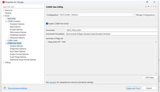
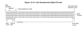
After readings on the spru513p guide, I adopted the intel format as the hex file to be parsed and transmitted to 79d, and the boot firmware will be writing or say programming the derived bytes into flash.
Question arises when populating the bytes to write Flash from the hex format image data. Some lines of the hex are not fullfilling 128 bits with some unfiled in the end. According to spnu629a guide for the FlashAPI on 2837xD device, which says:
Fapi_AutoEccGeneration – This mode will program the supplied data in Flash along with automatically generated ECC. The ECC is calculated for every 64-bit data aligned on a 64-bit memory boundary. Hence, when using this mode, all the 64 bits of the data should be programmed at the same time for a given 64-bit aligned memory address. Data not supplied is treated as all 1s (0xFFFF).
So my interpretation is, if there are unfilled bytes in the hex data, I should populate all 1s (e.g. FF) . Below are some example lines I got from the application hex file:
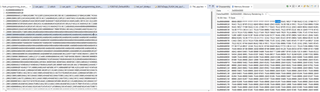
example 1 :140BA800003301000254880A10F0540A910A0000A80A000072
So based on the intel hex format definition, exclude the first 8 hex numbers, (number of bytes, address, type) and last 2 hex (CRC), this line has 14 ie. 20 bytes, the bytes to write to flash are (I aligend the representation below by every 128 bit i.e 8 * 16-bit hex)
"0033 0100 0254 880A 10F0 540A 910A"
"0000 A80A 0000 FFFF FFFF FFFF FFFF"
example 2 :1F0B8800061F22C029681A4AA8A5A4CDA6034A5A0622052EC4021A0625002500010606AF
This line has 1F i.e. 31 bytes, so my interpretation is
"061F 22C0 2968 1A4A A8A5 A4CD A603 4A5A"
"0622 052E C402 1A06 2500 2500 0106 06FF"
The FF with background color is what should be writen to the Flash.
Please don't bother with the detailed numbers, is my interpretation correct regarding the FF padding part?
Thanks for your suggestions in advance.
Regards,
Wei
Besides above, I also have question regarding the crespondancy between the hex file vs. the byte content in the Flash memory.
I generated intel hex from a ledblink project, and also opened the Memory view within CCS under debug mode of the exact project.
Below is the figure showing the two:
In the left is the generated hex file. Taking the 2nd line (whch contains data) as example:
:020000004A892B
according to the intel hex file format definition, my understanding is, from the begining to end, 02 stands for the number of bytes; 0000 is the address (to be combined with the base address in the 1st line, to form the 32bit address 000A0000); then 00 stands for a record of DATA, 4A 89 are the data which are 2 bytes, and 2B is CRC.
while in the memory view, as you can see in the RHS, at address 0x0000A000, it shows
004A 0B89 .....
I believe the 4A 89 are the data reflected in the line of the Hex file, but I am not sure why the 00, 0B was there, and where they comes from or recorded. If continue to look at data in rest of lines of the .hex, and compare that to the memory view, it also same pattern.
How to understand this, and how we should program the flash correctly? (I assume the flash programmed should match exactly what shown in the memory view, correct me if I am wrong.)
Thanks for advice.
Regards,
Wei
Wei,
Yes, each of the partial 128-bit memory aligned data should be padded with all 1s if you pass the data length as 8 for the program command when using Fapi_AutoEccGeneration.
Hope all of the initialized sections are aligned on 128-bit address in your linker command file using ALIGN(8).
Thanks and regards,
Vamsi
Thanks Vamsi.
Beside, I realized that the generated hex files actually has 2: app.hex and app.i01 (taking intel hex for example). By compare their content with the memory view, it's easy to find that, the 2 files contain the high / low byte, respectively.
Not sure if I missed something, Is there some settings in the hex output format option or so, that I can let CCS generate only 1 hex file to contain the image, not splitting into 2?
Regards,
Wei
Hi Wei,
What is the exact command that you used to generate the hex file?
Thanks and regards,
Vamsi
Hey Vamsi,
I generated the hex file with the CCS built-in:
And then, found the 2 files under the <build_configuration> folder: (.hex and .i01)
Regards,
Wei
Hi Wei,
We can review and get back to you next week.
Thanks and regards,
Vamsi
Hi Wei,
Do you have page0 and page1 in your linker command file? C2000 Hex utility generates separate hex files for page0 and page1. If you want to generate single hex file, map any initialized sections in your linker command file to page0 memories instead of page1.
Thanks and regards,
Vamsi
Thanks Vamsi. Yep I ahve page0 and page1 both used in the linker command file.
The 2 separate hex files is not a concern to me now. But for my curiousity, for example, my linker command file's page0/1 allocation looks looks like:
So if I want to generate single hex file, I need to fit all sections currently allocated in PAGE 1 to RAM/Flash in PAGE 0, for example:
.stack : > RAMM1 PAGE = 1
modify to things like
.stack : > RAMGS0 PAGE = 0
is my understanding correct? Thanks,
Regards,,
Wei
MEMORY { PAGE 0: /* Program Memory */ /* Memory (RAM/FLASH) blocks can be moved to PAGE1 for data allocation */ /* BEGIN is used for the "boot to Flash" bootloader mode */ BEGIN : origin = 0x080000, length = 0x000002 RAMM0 : origin = 0x000122, length = 0x0002DE RAMD0 : origin = 0x00B000, length = 0x000800 RAMLS03 : origin = 0x008000, length = 0x002000 /* RAMLS1 : origin = 0x008800, length = 0x000800 RAMLS2 : origin = 0x009000, length = 0x000800 RAMLS3 : origin = 0x009800, length = 0x000800 */ RAMLS4 : origin = 0x00A000, length = 0x000800 RESET : origin = 0x3FFFC0, length = 0x000002 /* Flash sectors */ FLASHA : origin = 0x080002, length = 0x001FFE /* on-chip Flash */ FLASHB : origin = 0x082000, length = 0x002000 /* on-chip Flash */ ... .... PAGE 1 : /* Data Memory */ /* Memory (RAM/FLASH) blocks can be moved to PAGE0 for program allocation */ BOOT_RSVD : origin = 0x000002, length = 0x000121 /* Part of M0, BOOT rom will use this for stack */ RAMM1 : origin = 0x000400, length = 0x0003F8 /* on-chip RAM block M1 */ // RAMM1_RSVD : origin = 0x0007F8, length = 0x000008 /* Reserve and do not use for code as per the errata advisory "Memory: Prefetching Beyond Valid Memory" */ RAMD1 : origin = 0x00B800, length = 0x000800 RAMLS5 : origin = 0x00A800, length = 0x000800 RAMGS0 : origin = 0x00C000, length = 0x001000 RAMGS1 : origin = 0x00D000, length = 0x001000 .... } SECTIONS { /* Allocate program areas: */ .cinit : > FLASHD PAGE = 0 .pinit : > FLASHD, PAGE = 0 .text : >> FLASHD | FLASHE PAGE = 0 codestart : > BEGIN PAGE = 0 #ifdef __TI_COMPILER_VERSION__ #if __TI_COMPILER_VERSION__ >= 15009000 GROUP { .TI.ramfunc { -l F021_API_F2837xD_FPU32.lib} } LOAD = FLASHD, RUN = RAMLS03, LOAD_START(_RamfuncsLoadStart), LOAD_SIZE(_RamfuncsLoadSize), LOAD_END(_RamfuncsLoadEnd), RUN_START(_RamfuncsRunStart), RUN_SIZE(_RamfuncsRunSize), RUN_END(_RamfuncsRunEnd), PAGE = 0 #else GROUP { ramfuncs { -l F021_API_F2837xD_FPU32.lib} } LOAD = FLASHD, RUN = RAMLS03, LOAD_START(_RamfuncsLoadStart), LOAD_SIZE(_RamfuncsLoadSize), LOAD_END(_RamfuncsLoadEnd), RUN_START(_RamfuncsRunStart), RUN_SIZE(_RamfuncsRunSize), RUN_END(_RamfuncsRunEnd), PAGE = 0 #endif #endif /* Allocate uninitalized data sections: */ .stack : > RAMM1 PAGE = 1 .ebss : >> RAMLS5 | RAMGS0 | RAMGS1 PAGE = 1 .esysmem : > RAMLS5 PAGE = 1 /* Initalized sections go in Flash */ .econst : >> FLASHF | FLASHG PAGE = 0 .switch : > FLASHD PAGE = 0 .reset : > RESET, PAGE = 0, TYPE = DSECT /* not used, */ Filter_RegsFile : > RAMGS0, PAGE = 1 SHARERAMGS0 : > RAMGS0, PAGE = 1 SHARERAMGS1 : > RAMGS1, PAGE = 1 /* Flash Programming Buffer */ BufferDataSection : > RAMD1, PAGE = 1, ALIGN(8) }
Hi Wei,
C2000 memory is unified memory. There is no need of page0 and page1. You can define all the memories in Page0 and leave page1 empty if you want.
Page0/Page1 concept was left over because of legacy.
Thanks and regards,
Vamsi