Part Number: TMS320F28379D
Other Parts Discussed in Thread: SYSCONFIG, C2000WARE
Hello,
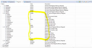
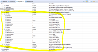
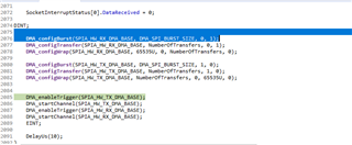
I am trying to retrieve ethernet data from a W5500 using the TMS320F28379D's SPI and DMA. Please see contents of my project's sysconfig file below.
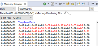
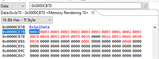
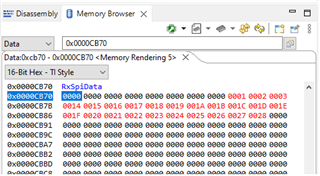
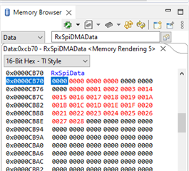
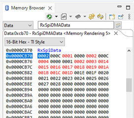
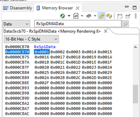
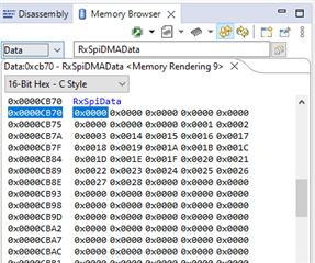
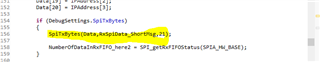
I can see the MISO data on the oscilloscope, however, I am not seeing the correct data in the Rx Buffer after the SPI Rx DMA's transfer complete interrupt occurs.
Also, the SPI Rx FIFO buffer still has data in it.
What is wrong with my SPI/DMA configuration.
Stephen
/**
* These arguments were used when this file was generated. They will be automatically applied on subsequent loads
* via the GUI or CLI. Run CLI with '--help' for additional information on how to override these arguments.
* @cliArgs --device "F2837xD" --package "F2837xD_337ZWT" --part "F2837xD_337ZWT" --context "CPU1" --product "C2000WARE@5.01.00.00"
* @versions {"tool":"1.18.0+3266"}
*/
/**
* Import the modules used in this configuration.
*/
const device_support = scripting.addModule("/driverlib/device_support.js");
const flash = scripting.addModule("/driverlib/flash.js", {}, false);
const flash1 = flash.addInstance();
const sci = scripting.addModule("/driverlib/sci.js", {}, false);
const sci1 = sci.addInstance();
const spi = scripting.addModule("/driverlib/spi.js", {}, false);
const spi1 = spi.addInstance();
const sysctl = scripting.addModule("/driverlib/sysctl.js");
const FREERTOS = scripting.addModule("/kernel/freertos_tool/FREERTOS", {}, false);
const FREERTOS1 = FREERTOS.addInstance();
/**
* Write custom configuration values to the imported modules.
*/
const divider4 = system.clockTree["LOSPCP"];
divider4.divideValue = 6;
const divider5 = system.clockTree["SYSCLKDIVSEL"];
divider5.divideValue = 1;
const multiplier4 = system.clockTree["PLL_IMULT"];
multiplier4.multiplyValue = 10;
const mux8 = system.clockTree["XTAL_OR_X1"];
mux8.inputSelect = "X1";
flash1.$name = "myFMC0";
flash1.enableECC = false;
sci1.useInterrupts = false;
sci1.$name = "mySCIB";
sci1.baudRates = 38400;
sci1.sci.$assign = "SCIB";
spi1.transferProtocol = "SPI_PROT_POL0PHA1";
spi1.$name = "SPIA_HW";
spi1.mode = "SPI_MODE_CONTROLLER";
spi1.bitRate = 6666666;
spi1.dataWidth = "8";
spi1.emulationMode = "SPI_EMULATION_STOP_AFTER_TRANSMIT";
spi1.useDMARX = true;
spi1.useDMATX = true;
spi1.registerInterrupts = true;
spi1.txFifo = "SPI_FIFO_TX8";
spi1.rxFifo = "SPI_FIFO_RX4";
spi1.enabledFIFOInterrupts = ["SPI_INT_RXFF"];
spi1.useInterrupts = false;
spi1.spi.$assign = "SPIA";
spi1.spiRXDMA.databusWidthConfig = scripting.forceWrite("DMA_CFG_SIZE_16BIT");
spi1.spiRXDMA.transferSize = 16;
spi1.spiRXDMA.burstSize = 8;
spi1.spiRXDMA.destAddressInputMode = "VARIABLE";
spi1.spiRXDMA.destAddressVariable = "RxSpiDMAData";
spi1.spiRXDMA.useInterrupts = true;
spi1.spiRXDMA.registerInterrupts = true;
spi1.spiRXDMA.enableInterrupts = true;
spi1.spiRXDMA.enableTriggers = true;
spi1.spiRXDMA.interruptMode = "DMA_INT_AT_END";
spi1.spiRXDMA.emulationMode = "DMA_EMULATION_FREE_RUN";
spi1.spiRXDMA.dmaInt.enableInterrupt = true;
spi1.spiTXDMA.databusWidthConfig = scripting.forceWrite("DMA_CFG_SIZE_16BIT");
spi1.spiTXDMA.dmaBase = "DMA_CH2_BASE";
spi1.spiTXDMA.srcAddressInputMode = "VARIABLE";
spi1.spiTXDMA.srcAddressVariable = "TxSpiDMAData";
spi1.spiTXDMA.burstSize = 8;
spi1.spiTXDMA.transferSize = 16;
spi1.spiTXDMA.useInterrupts = true;
spi1.spiTXDMA.registerInterrupts = true;
spi1.spiTXDMA.enableInterrupts = true;
spi1.spiTXDMA.enableTriggers = true;
spi1.spiTXDMA.interruptMode = "DMA_INT_AT_END";
spi1.spiTXDMA.dmaInt.enableInterrupt = true;
sysctl.enable_SYSCTL_PERIPH_CLK_CLA1 = false;
sysctl.enable_SYSCTL_PERIPH_CLK_HRPWM = false;
sysctl.enable_SYSCTL_PERIPH_CLK_EMIF1 = false;
sysctl.enable_SYSCTL_PERIPH_CLK_EMIF2 = false;
sysctl.enable_SYSCTL_PERIPH_CLK_EPWM1 = false;
sysctl.enable_SYSCTL_PERIPH_CLK_EPWM2 = false;
sysctl.enable_SYSCTL_PERIPH_CLK_EPWM3 = false;
sysctl.enable_SYSCTL_PERIPH_CLK_EPWM4 = false;
sysctl.enable_SYSCTL_PERIPH_CLK_EPWM5 = false;
sysctl.enable_SYSCTL_PERIPH_CLK_EPWM6 = false;
sysctl.enable_SYSCTL_PERIPH_CLK_EPWM7 = false;
sysctl.enable_SYSCTL_PERIPH_CLK_EPWM8 = false;
sysctl.enable_SYSCTL_PERIPH_CLK_EPWM9 = false;
sysctl.enable_SYSCTL_PERIPH_CLK_EPWM10 = false;
sysctl.enable_SYSCTL_PERIPH_CLK_EPWM11 = false;
sysctl.enable_SYSCTL_PERIPH_CLK_EPWM12 = false;
sysctl.enable_SYSCTL_PERIPH_CLK_ECAP1 = false;
sysctl.enable_SYSCTL_PERIPH_CLK_ECAP2 = false;
sysctl.enable_SYSCTL_PERIPH_CLK_ECAP3 = false;
sysctl.enable_SYSCTL_PERIPH_CLK_ECAP4 = false;
sysctl.enable_SYSCTL_PERIPH_CLK_ECAP5 = false;
sysctl.enable_SYSCTL_PERIPH_CLK_ECAP6 = false;
sysctl.enable_SYSCTL_PERIPH_CLK_EQEP1 = false;
sysctl.enable_SYSCTL_PERIPH_CLK_EQEP2 = false;
sysctl.enable_SYSCTL_PERIPH_CLK_EQEP3 = false;
sysctl.enable_SYSCTL_PERIPH_CLK_SD1 = false;
sysctl.enable_SYSCTL_PERIPH_CLK_SD2 = false;
sysctl.enable_SYSCTL_PERIPH_CLK_SCIA = false;
sysctl.enable_SYSCTL_PERIPH_CLK_SCIC = false;
sysctl.enable_SYSCTL_PERIPH_CLK_SCIB = false;
sysctl.enable_SYSCTL_PERIPH_CLK_SCID = false;
sysctl.enable_SYSCTL_PERIPH_CLK_SPIB = false;
sysctl.enable_SYSCTL_PERIPH_CLK_SPIC = false;
sysctl.enable_SYSCTL_PERIPH_CLK_I2CA = false;
sysctl.enable_SYSCTL_PERIPH_CLK_I2CB = false;
sysctl.enable_SYSCTL_PERIPH_CLK_CANA = false;
sysctl.enable_SYSCTL_PERIPH_CLK_CANB = false;
sysctl.enable_SYSCTL_PERIPH_CLK_MCBSPA = false;
sysctl.enable_SYSCTL_PERIPH_CLK_MCBSPB = false;
sysctl.enable_SYSCTL_PERIPH_CLK_UPPA = false;
sysctl.enable_SYSCTL_PERIPH_CLK_USBA = false;
sysctl.enable_SYSCTL_PERIPH_CLK_ADCA = false;
sysctl.enable_SYSCTL_PERIPH_CLK_ADCB = false;
sysctl.enable_SYSCTL_PERIPH_CLK_ADCD = false;
sysctl.enable_SYSCTL_PERIPH_CLK_ADCC = false;
sysctl.enable_SYSCTL_PERIPH_CLK_CMPSS1 = false;
sysctl.enable_SYSCTL_PERIPH_CLK_CMPSS3 = false;
sysctl.enable_SYSCTL_PERIPH_CLK_CMPSS4 = false;
sysctl.enable_SYSCTL_PERIPH_CLK_CMPSS2 = false;
sysctl.enable_SYSCTL_PERIPH_CLK_CMPSS5 = false;
sysctl.enable_SYSCTL_PERIPH_CLK_CMPSS6 = false;
sysctl.enable_SYSCTL_PERIPH_CLK_CMPSS7 = false;
sysctl.enable_SYSCTL_PERIPH_CLK_CMPSS8 = false;
sysctl.enable_SYSCTL_PERIPH_CLK_DACA = false;
sysctl.enable_SYSCTL_PERIPH_CLK_DACB = false;
sysctl.enable_SYSCTL_PERIPH_CLK_DACC = false;
sysctl.secControllerFrame2 = "SYSCTL_SEC_CONTROLLER_DMA";
sysctl.secControllerFrame1 = "SYSCTL_SEC_CONTROLLER_DMA";
FREERTOS1.$name = "myFREERTOS0";
FREERTOS1.MINIMAL_STACK_SIZE = 256;
FREERTOS1.CPU_CLOCK_HZ = 200000000;
FREERTOS1.tasks.create(1);
FREERTOS1.tasks[0].taskPointer = "Task_4ms";
FREERTOS1.tasks[0].$name = "TASK_4milliseconds";
FREERTOS1.tasks[0].taskStackSize = 1300;
FREERTOS1.tasks[0].taskPriority = 18;
FREERTOS1.semaphores.create(2);
FREERTOS1.semaphores[0].$name = "Task100ms_binarySem1";
FREERTOS1.semaphores[1].$name = "Task10ms_binarySem1";
/**
* Pinmux solution for unlocked pins/peripherals. This ensures that minor changes to the automatic solver in a future
* version of the tool will not impact the pinmux you originally saw. These lines can be completely deleted in order to
* re-solve from scratch.
*/
sci1.sci.scirxdPin.$suggestSolution = "GPIO11";
sci1.sci.scitxdPin.$suggestSolution = "GPIO10";
spi1.spi.spi_picoPin.$suggestSolution = "GPIO16";
spi1.spi.spi_pociPin.$suggestSolution = "GPIO17";
spi1.spi.spi_clkPin.$suggestSolution = "GPIO18";
spi1.spi.spi_ptePin.$suggestSolution = "GPIO19";