This thread has been locked.

If you have a related question, please click the "Ask a related question" button in the top right corner. The newly created question will be automatically linked to this question.

TMS320F2800157: How to modify the drv8323rs code to apply to drv8323rh?

Part Number: TMS320F2800157
Other Parts Discussed in Thread: DRV8300, BOOSTXL-DRV8323RS, LAUNCHXL-F280025C, LAUNCHXL-F2800157

Hi,

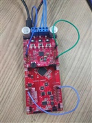
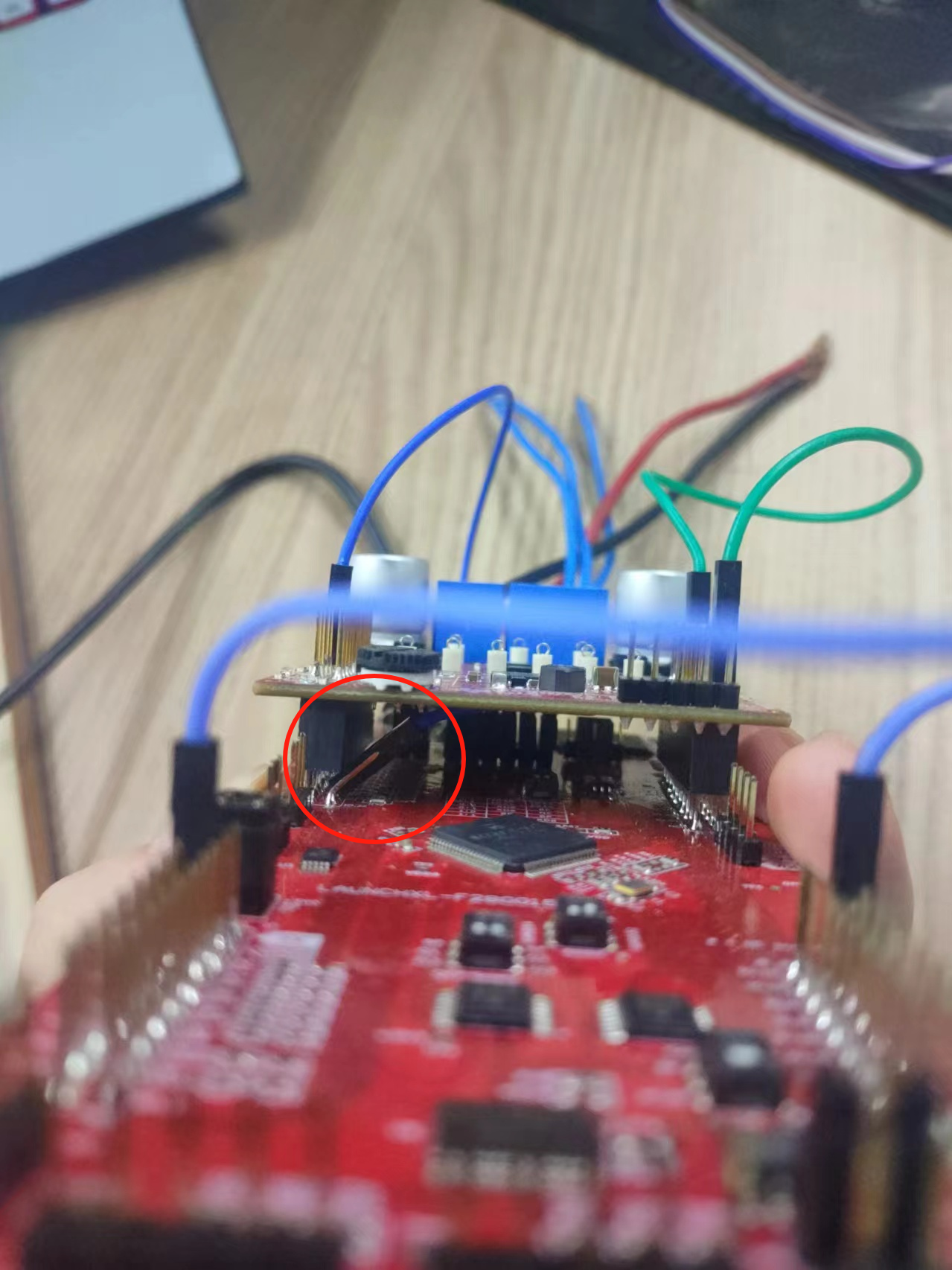
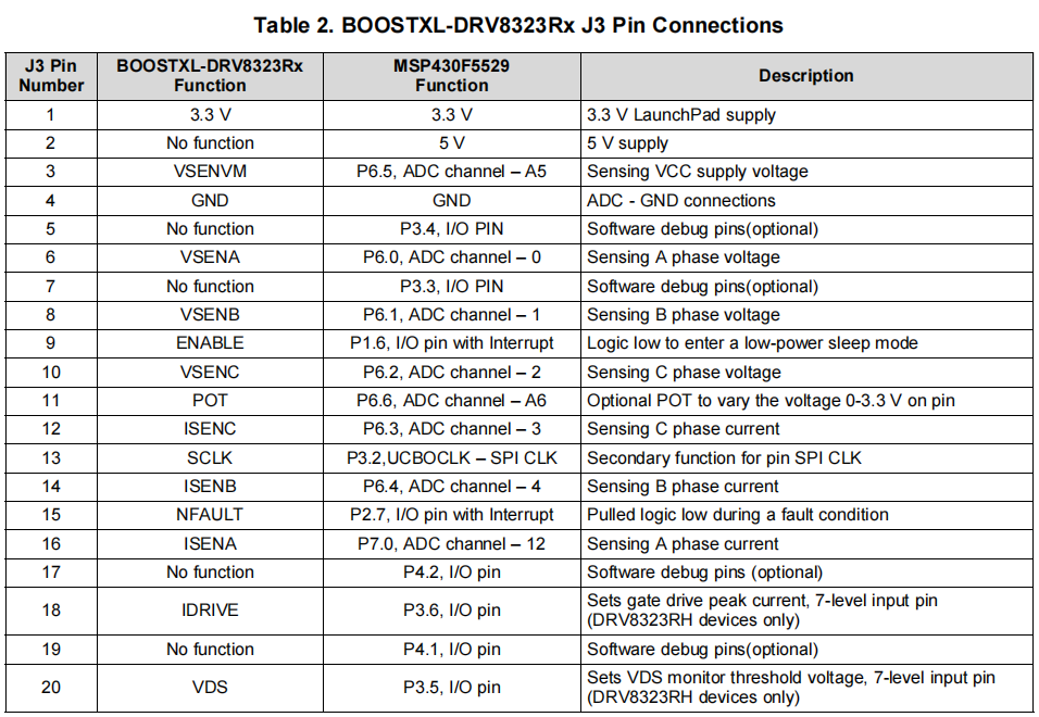
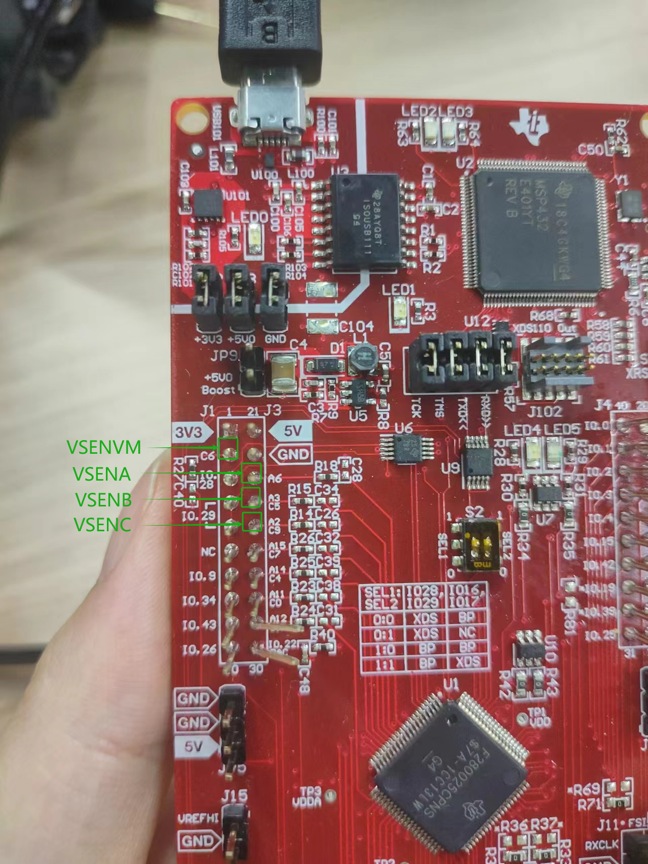
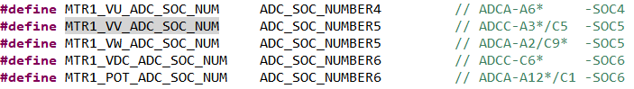
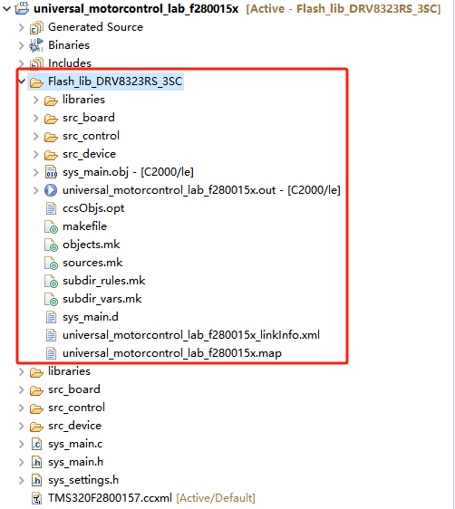
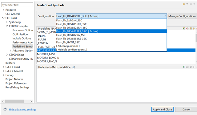
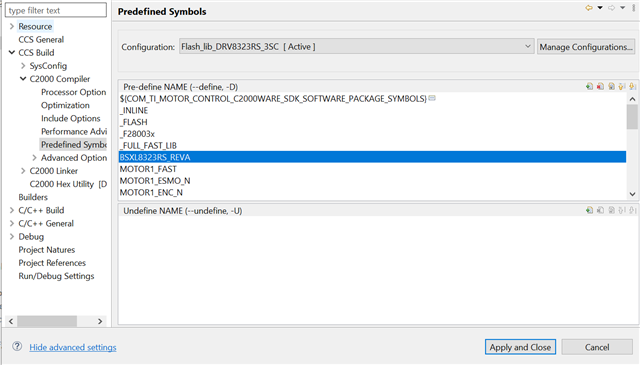
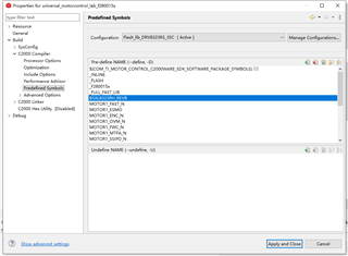
I need to use F280015x+DRV8300 for the final product. Currently, the official routine of F280015x only includes the routine of DRV8323RS. I think I should configure the case of F280015x+DRV8323RH first. Found that DRV8323RS and DRV8323RH code has a big difference, and modify the configuration is a key modification, I do not know its specific operation, can you teach me how to modify the F280015x+DRV8323RS routine, so that it can be used in the configuration of F280015x+DRV8323RH?

Thank you for any help!

Regards,

Johnny

  • Hello Johnny!

    Apologies for the delay, I was taking the time to write out a comprehensive answer. When it comes to a difference in HW drivers, the easiest way to begin is by looking at the difference in what is being driven.

    Pull the datasheet for the DRV8323Rx from the product page: https://www.ti.com/product/DRV8323R. Section 8.3.1.2 Device Interface Modes describes our two options. The DRV8323RS uses the SPI, while the -H uses the Hardware Interface.

    Look at figure 23 and 24.

    When using the Hardware Interface, the Gain, Idrive, Mode, and VDS signals, which are set by hardware, replace the SPI's SCLK, SDI, SDO, and nSCS signals. Of course, there's also not SPI communication with the DRV at all.

    So, what does this mean for our firmware?

    All instances of SPI communication (read or write) to the DRV must be disabled and/or removed, as this is no longer present.

    1. Using CCS' Ctrl+H C-code search feature, search for " *DRV* "

    2. For the most part, this is all DRV-related firmware in the project. Any time you see the words "read" or "write", determine if this needs to be removed.
      1. As one example, in sys_main.c, there's a function call to "HAL_readDRVData(...)" . This call should be disabled and/or removed.

    3. Search specifically for " *DRVIC* "
      1. These are all function calls to the DRV firmware. Any time these utilizes SPI communication, the SPI communication should be disabled or removed.

    4. All instances of configuring the SPI for DRV communication must be disabled and/or removed.
      1. Using the search feature, search for " *SPI* "
      2. This is all SPI configuration-related code in the project. This is both DRV configuration and DAC configuration. Leave the DAC configuration alone!
        1. The following functions should be specifically looked at:
          1. HAL_setupDRVSPI(...) configures the SPI in DRV mode.
          2. HAL_setupSPI(...) only needs to be called once, in HAL_MTR_setParams(...). The call in sys_main.c can be removed.
        2. Review the other search results and determine what's related to the DRV and the DAC- usually, you can tell by the naming convention.

    5. All side effects of SPI communication to the DRV (for example, SPI-based fault reading, if present) must be disabled and/or removed.

    6. The GPIO configuration for the SPI is set up to alternate between the DRV and the DAC. This can be removed, instead only allowing DAC communication.

    Hope that makes sense!

    Regards,
    Jason Osborn

  • Hi Jason,

    Thank you very much!Your advice points me in the right direction,but I tried to find that there is still a problem, I do not know whether my operation is wrong, my operation is as follows.

    1.Change the predefined symbol "BSXL8323RS_REVA" in the official routine properties of F280015x+DRV8323RS to "BSXL8323RH_REVB".

    2.Modify the I/O port configuration of the F280015x+RS by referring to the I/O port configuration of J1, J2, J3, and J4 in the F280013x official routine RS and RH configuration.


    #elif defined(BSXL8323RH_REVB)
        // GPIO30->EPWM1A->M1_UH*
        GPIO_setPinConfig(GPIO_30_EPWM1_A);
        GPIO_setDirectionMode(30, GPIO_DIR_MODE_OUT);
        GPIO_setPadConfig(30, GPIO_PIN_TYPE_STD);
    
        // GPIO1->EPWM1B->M1_UL*
        GPIO_setPinConfig(GPIO_1_EPWM1_B);
        GPIO_setDirectionMode(1, GPIO_DIR_MODE_OUT);
        GPIO_setPadConfig(1, GPIO_PIN_TYPE_STD);
    
        // GPIO2->EPWM2A->M1_VH*
        GPIO_setPinConfig(GPIO_2_EPWM2_A);
        GPIO_setDirectionMode(2, GPIO_DIR_MODE_OUT);
        GPIO_setPadConfig(2, GPIO_PIN_TYPE_STD);
    
        // GPIO3->EPWM2B->M1_VL*
        GPIO_setPinConfig(GPIO_3_EPWM2_B);
        GPIO_setDirectionMode(3, GPIO_DIR_MODE_OUT);
        GPIO_setPadConfig(3, GPIO_PIN_TYPE_STD);
    
    #if defined(CMD_CAN_EN)
        // GPIO4->CANA_TX
        GPIO_setPinConfig(GPIO_4_CANA_TX);
        GPIO_setDirectionMode(4, GPIO_DIR_MODE_OUT);
        GPIO_setPadConfig(4, GPIO_PIN_TYPE_STD);
    
        // GPIO5->CANA_RX
        GPIO_setPinConfig(GPIO_5_CANA_RX);
        GPIO_setDirectionMode(5, GPIO_DIR_MODE_IN);
        GPIO_setPadConfig(5, GPIO_PIN_TYPE_STD);
    #elif defined(DAC128S_ENABLE)
        // GPIO4->Reserve
        GPIO_setPinConfig(GPIO_4_GPIO4);
        GPIO_setDirectionMode(4, GPIO_DIR_MODE_IN);
        GPIO_setPadConfig(4, GPIO_PIN_TYPE_STD);
    
        // GPIO11->SPIA_STE
        //GPIO_setPinConfig(GPIO_11_SPIA_STE);
        GPIO_setPinConfig(GPIO_11_GPIO11);
        GPIO_setDirectionMode(11, GPIO_DIR_MODE_IN);
        GPIO_setPadConfig(11, GPIO_PIN_TYPE_STD);
    #else
        // GPIO4->Reserve
        GPIO_setPinConfig(GPIO_4_GPIO4);
        GPIO_setDirectionMode(4, GPIO_DIR_MODE_IN);
        GPIO_setPadConfig(4, GPIO_PIN_TYPE_STD);
    
        // GPIO5->Reserve
        GPIO_setPinConfig(GPIO_5_GPIO5);
        GPIO_setDirectionMode(5, GPIO_DIR_MODE_IN);
        GPIO_setPadConfig(5, GPIO_PIN_TYPE_STD);
    #endif   // !CMD_CAN_EN
    
    
        // GPIO7->Reserve
        GPIO_setPinConfig(GPIO_7_GPIO7);
        GPIO_setDirectionMode(7, GPIO_DIR_MODE_IN);
        GPIO_setPadConfig(7, GPIO_PIN_TYPE_STD);
    
        // GPIO8->SPIA_SIMO->M1_DRV_SDI/DAC128S_SDI
        GPIO_setPinConfig(GPIO_8_SPIA_SIMO);
        GPIO_setDirectionMode(8, GPIO_DIR_MODE_OUT);
        GPIO_setPadConfig(8, GPIO_PIN_TYPE_STD);
    
        // GPIO09->SPIA_CLK->M1_DRV_SCLK/DAC128S_SCLK
        GPIO_setPinConfig(GPIO_9_SPIA_CLK);
        GPIO_setDirectionMode(9, GPIO_DIR_MODE_OUT);
        GPIO_setPadConfig(9, GPIO_PIN_TYPE_PULLUP);
    
        // GPIO0->EPWM3_A
        GPIO_setPinConfig(GPIO_0_EPWM3_A);
        GPIO_setDirectionMode(0, GPIO_DIR_MODE_OUT);
        GPIO_setPadConfig(0, GPIO_PIN_TYPE_STD);
    
        // GPIO15->EPWM3_B
        GPIO_setPinConfig(GPIO_15_EPWM3_B);
        GPIO_setDirectionMode(15, GPIO_DIR_MODE_OUT);
        GPIO_setPadConfig(15, GPIO_PIN_TYPE_STD);
    
        // GPIO12->Reserve
        GPIO_setPinConfig(GPIO_12_GPIO12);
        GPIO_setDirectionMode(12, GPIO_DIR_MODE_OUT);
        GPIO_setPadConfig(12, GPIO_PIN_TYPE_STD);
    #if defined(MOTOR1_HALL)
        // GPIO14->HALL_U
        GPIO_setPinConfig(GPIO_14_GPIO14);
        GPIO_setDirectionMode(14, GPIO_DIR_MODE_IN);
        GPIO_setPadConfig(14, GPIO_PIN_TYPE_STD);
        GPIO_setQualificationMode(14, GPIO_QUAL_3SAMPLE);
        GPIO_setQualificationPeriod(14, 4);
    
        // GPIO26->HALL_W
        GPIO_setPinConfig(GPIO_26_GPIO26);
        GPIO_setDirectionMode(26, GPIO_DIR_MODE_IN);
        GPIO_setPadConfig(26, GPIO_PIN_TYPE_STD);
        GPIO_setQualificationMode(26, GPIO_QUAL_3SAMPLE);
        GPIO_setQualificationPeriod(26, 2);
    
        // GPIO33->HALL_V
        GPIO_setPinConfig(GPIO_33_GPIO33);
        GPIO_setDirectionMode(33, GPIO_DIR_MODE_IN);
        GPIO_setPadConfig(33, GPIO_PIN_TYPE_STD);
        GPIO_setQualificationMode(33, GPIO_QUAL_3SAMPLE);
        GPIO_setQualificationPeriod(33, 2);
    #else
     // GPIO26->M1_DRV_nSCS/GAIN (has a 47k pull down), jump to J2-19
        GPIO_setPinConfig(GPIO_26_GPIO26);
        GPIO_setDirectionMode(26, GPIO_DIR_MODE_IN);
        GPIO_setPadConfig(26, GPIO_PIN_TYPE_STD);
    
      // GPIO33->M1_DRV_CAL, Low->Disable
        GPIO_setPinConfig(GPIO_33_GPIO33);
        GPIO_writePin(33, 0);
        GPIO_setDirectionMode(33, GPIO_DIR_MODE_OUT);
        GPIO_setPadConfig(33, GPIO_PIN_TYPE_STD);
    #endif   // !MOTOR1_HALL
    
        // GPIO16->Reserve
        GPIO_setPinConfig(GPIO_16_GPIO16);
        GPIO_setDirectionMode(16, GPIO_DIR_MODE_IN);
        GPIO_setPadConfig(16, GPIO_PIN_TYPE_STD);
    
        // GPIO10->SPIA_SOMI->DRV_SDO/DAC_SDO
        GPIO_setPinConfig(GPIO_10_SPIA_SOMI);
        GPIO_setDirectionMode(10, GPIO_DIR_MODE_IN);
        GPIO_setPadConfig(10, GPIO_PIN_TYPE_STD);
    
        // GPIO18->Reserve
        GPIO_setPinConfig(GPIO_18_GPIO18);
        GPIO_setDirectionMode(18, GPIO_DIR_MODE_IN);
        GPIO_setPadConfig(18, GPIO_PIN_TYPE_STD);
    
        // GPIO34->DAC128S_SYNC (Switch needed), Jump from JB-2/JA-2********Reserve
        GPIO_setPinConfig(GPIO_34_GPIO34);
        //GPIO_writePin(34, 1);
        //GPIO_setDirectionMode(34, GPIO_DIR_MODE_OUT);
        GPIO_setDirectionMode(34, GPIO_DIR_MODE_IN);
        GPIO_setPadConfig(34, GPIO_PIN_TYPE_STD);
    
        // GPIO35->M1_DRV_LED
        GPIO_setPinConfig(GPIO_35_GPIO35);
        GPIO_writePin(35, 1);
        GPIO_setDirectionMode(35, GPIO_DIR_MODE_OUT);
        GPIO_setPadConfig(35, GPIO_PIN_TYPE_STD);
    
    
        // GPIO24->M1_DRV_nFAULT
        GPIO_setPinConfig(GPIO_24_GPIO24);
        GPIO_setDirectionMode(24, GPIO_DIR_MODE_IN);
        GPIO_setPadConfig(24, GPIO_PIN_TYPE_PULLUP);
        GPIO_setQualificationMode(24, GPIO_QUAL_3SAMPLE);
        GPIO_setQualificationPeriod(24, 2);
    
        // GPIO28->HAL_GPIO_ISR_M1
        GPIO_setPinConfig(GPIO_28_GPIO28);
        GPIO_writePin(28, 1);
        GPIO_setDirectionMode(28, GPIO_DIR_MODE_OUT);
        GPIO_setPadConfig(28, GPIO_PIN_TYPE_PULLUP);
    
        // GPIO29->M1_DRV_ENABLE*
        GPIO_setPinConfig(GPIO_29_GPIO29);
        GPIO_writePin(29, 1);
        GPIO_setDirectionMode(29, GPIO_DIR_MODE_OUT);
        GPIO_setPadConfig(29, GPIO_PIN_TYPE_PULLUP);
    
        // GPIO32->Reserve
        GPIO_setPinConfig(GPIO_32_GPIO32);
        GPIO_setDirectionMode(32, GPIO_DIR_MODE_IN);
        GPIO_setPadConfig(32, GPIO_PIN_TYPE_STD);
    
        // GPIO37->SPIA_STE->M1_DAC_SCS,
        GPIO_setPinConfig(GPIO_37_SPIA_STE);
        GPIO_writePin(37, 1);
        GPIO_setDirectionMode(37, GPIO_DIR_MODE_OUT);
        GPIO_setPadConfig(37, GPIO_PIN_TYPE_STD);
    
        // GPIO43->EQEP1_INDEX
        GPIO_setPinConfig(GPIO_43_EQEP1_INDEX);
        GPIO_setDirectionMode(43, GPIO_DIR_MODE_IN);
        GPIO_setPadConfig(43, GPIO_PIN_TYPE_STD);
        GPIO_setQualificationMode(43, GPIO_QUAL_3SAMPLE);
        GPIO_setQualificationPeriod(43, 2);
    
        // GPIO20->EQEP1_A
        GPIO_setPinConfig(GPIO_20_EQEP1_A);
        GPIO_setDirectionMode(20, GPIO_DIR_MODE_IN);
        GPIO_setPadConfig(20, GPIO_PIN_TYPE_STD);
        GPIO_setQualificationMode(20, GPIO_QUAL_3SAMPLE);
        GPIO_setQualificationPeriod(20, 2);
    
        // GPIO21->EQEP1_B
        GPIO_setPinConfig(GPIO_21_EQEP1_B);
        GPIO_setDirectionMode(21, GPIO_DIR_MODE_IN);
        GPIO_setPadConfig(21, GPIO_PIN_TYPE_STD);
        GPIO_setQualificationMode(21, GPIO_QUAL_3SAMPLE);
        GPIO_setQualificationPeriod(21, 2);
    
        // GPIO44->Reserve(add)
    #if defined(DAC128S_ENABLE)
        GPIO_setPinConfig(GPIO_44_GPIO44);
        GPIO_setDirectionMode(44, GPIO_DIR_MODE_OUT);
        GPIO_setPadConfig(44, GPIO_PIN_TYPE_STD);
    #endif
        // end of BSXL8323RH_REVB

    3.After compiling, modify the program code according to the error.(Most of them lack RH related functions)

        a.Add RH-related structs in the typedef struct _HAL_MTR_Obj_ of the "hal_obj.h" file

            On line 147:

    #elif defined(BSXL8323RH_REVB)
      uint32_t       gateEnableGPIO;
      uint32_t       gateModeGPIO;
      uint32_t       gateGainGPIO;
      uint32_t       gateCalGPIO;
      // BSXL8323RH_REVB

        b.Add RH-related code to the "hal.h" file.

            On line 693:

    //------------------------------------------------------------------------------
    #elif defined(BSXL8323RH_REVB)
    //------------------------------------------------------------------------------
    #define COM_CAN_BASE                    CANA_BASE
    
    #define COM_CANRX_GPIO                  5
    #define COM_CANTX_GPIO                  4
    
    #define COM_CANRX_GPIO_PIN_CONFIG       GPIO_5_CANA_RX
    #define COM_CANTX_GPIO_PIN_CONFIG       GPIO_4_CANA_TX
    
    #define COM_INT_CAN                     INT_CANA0
    
    #define GUI_SCI_BASE                    SCIA_BASE
    
    #define GUI_SCI_SCIRX_GPIO              28
    #define GUI_SCI_SCITX_GPIO              29
    
    #define GUI_SCI_SCIRX_PIN_CONFIG        GPIO_28_SCIA_RX
    #define GUI_SCI_SCITX_PIN_CONFIG        GPIO_29_SCIA_TX
    
    #define GUI_LED_GPIO                    20
    #define GUI_LED_GPIO_GPIO_PIN_CONFIG    GPIO_20_GPIO20
    
    //------------------------------------------------------------------------------
    #define EPWMDAC1_BASE           EPWM4_BASE      // N/A, on site_2
    #define EPWMDAC2_BASE           EPWM4_BASE      // N/A, on site_2
    #define EPWMDAC3_BASE           EPWM5_BASE      // N/A, on site_2
    #define EPWMDAC4_BASE           EPWM5_BASE      // N/A, on site_2
    
    // Install the boostxlPak or EVM on site 1 (near emulator) on launchPad
    //! \ Motor 1
    #define MTR1_PWM_U_BASE         EPWM1_BASE
    #define MTR1_PWM_V_BASE         EPWM2_BASE
    #define MTR1_PWM_W_BASE         EPWM3_BASE
    
    // Install the boostxlPak or EVM on site 1 (near emulator) on launchPad
    #define MTR1_PWM_U_BASE         EPWM1_BASE
    #define MTR1_PWM_V_BASE         EPWM2_BASE
    #define MTR1_PWM_W_BASE         EPWM3_BASE
    
    //! \brief Defines the gpio for enabling Power Module
    #define MTR1_GATE_EN_GPIO       29                  // N/A
    
    //! \brief Defines the gpio for the nFAULT of Power Module
    #define MTR1_PM_nFAULT_GPIO     24
    
    //! \brief Defines the gpio for calibration
    #define MTR1_GATE_CAL_GPIO      33
    
    //! \brief Defines the gpio for setting gain
    #define MTR1_GATE_GAIN_GPIO    26
    
    //! \brief Defines the gpio for setting mode
    #define MTR1_GATE_MODE_GPIO     48
    
    // QEP for encoder
    #define MTR1_QEP_BASE           EQEP1_BASE
    
    #define MTR1_HALL_U_GPIO        14
    #define MTR1_HALL_V_GPIO        33
    #define MTR1_HALL_W_GPIO        26
    
    
    #if defined(MOTOR1_HALL) && defined(CMD_CAP_EN)
    #error HALL and CMD_CAP can't be enabled at the same time
    #elif defined(MOTOR1_HALL)
    #define MTR1_CAP_U_BASE         ECAP1_BASE
    #define MTR1_CAP_V_BASE         ECAP2_BASE
    #define MTR1_CAP_W_BASE         ECAP3_BASE
    
    #define MTR1_CAP_U_XBAR         XBAR_INPUT4
    #define MTR1_CAP_V_XBAR         XBAR_INPUT5
    #define MTR1_CAP_W_XBAR         XBAR_INPUT6
    
    #define MTR1_CAP_U_INSEL        ECAP_INPUT_INPUTXBAR4
    #define MTR1_CAP_V_INSEL        ECAP_INPUT_INPUTXBAR5
    #define MTR1_CAP_W_INSEL        ECAP_INPUT_INPUTXBAR6
    
    #elif defined(CMD_CAP_EN)
    #define MTR1_CAP_FREQ_GPIO      40
    #define MTR1_CAP_FREQ_BASE      ECAP1_BASE
    #define MTR1_CAP_FREQ_XBAR      XBAR_INPUT4
    #define MTR1_CAP_FREQ_INSEL     ECAP_INPUT_INPUTXBAR4
    #endif  // CMD_CAP_EN
    
    #if defined(CMD_SWITCH_EN)
    #define MTR1_CMD_SWITCH_GPIO    23
    #define MTR1_CMD_STATE_GPIO     35
    #endif  // CMD_SWITCH_EN
    
    // XBAR-EPWM
    #define MTR1_XBAR_TRIP_ADDRL    XBAR_O_TRIP7MUX0TO15CFG
    #define MTR1_XBAR_TRIP_ADDRH    XBAR_O_TRIP7MUX16TO31CFG
    
    
    // TZ
    #define MTR1_XBAR_INPUT1        XBAR_INPUT1
    #define MTR1_TZ_OSHT1           EPWM_TZ_SIGNAL_OSHT1
    
    #define MTR1_XBAR_TRIP          XBAR_TRIP7
    #define MTR1_DCTRIPIN           EPWM_DC_COMBINATIONAL_TRIPIN7
    
    #define MTR1_CMPSS_DACH_VALUE   (2048 + 1024 + 512)
    #define MTR1_CMPSS_DACL_VALUE   (2048 - 1024 - 512)
    
    //! \brief Defines the PWM deadband falling edge delay count (system clocks)
    #define MTR1_PWM_DBFED_CNT      5           // 50ns
    
    //! \brief Defines the PWM deadband rising edge delay count (system clocks)
    #define MTR1_PWM_DBRED_CNT      5           // 50ns
    
    #if defined(MOTOR1_DCLINKSS)    // Single Shunt
    // Single-shunt
    
    // ADC & CMPSS
    #define MTR1_ADC_TRIGGER_SOC         ADC_TRIGGER_EPWM1_SOCA  // EPWM1_SOCA
    #define MTR1_ADC_I_SAMPLEWINDOW     14
    #define MTR1_ADC_V_SAMPLEWINDOW     20
    
    #if defined(FAST_DCLINKSS)
    #define MTR1_IDC1_TRIGGER_SOC    ADC_TRIGGER_EPWM6_SOCA  // EPWM6_SOCA
    #define MTR1_IDC2_TRIGGER_SOC    ADC_TRIGGER_EPWM6_SOCA  // EPWM6_SOCA
    #define MTR1_IDC3_TRIGGER_SOC    ADC_TRIGGER_EPWM6_SOCB  // EPWM6_SOCB
    #define MTR1_IDC4_TRIGGER_SOC    ADC_TRIGGER_EPWM6_SOCB  // EPWM6_SOCB
    #else   // !FAST_DCLINKSS
    #define MTR1_IDC1_TRIGGER_SOC    ADC_TRIGGER_EPWM2_SOCA  // EPWM2_SOCA
    #define MTR1_IDC2_TRIGGER_SOC    ADC_TRIGGER_EPWM2_SOCB  // EPWM2_SOCB
    #define MTR1_IDC3_TRIGGER_SOC    ADC_TRIGGER_EPWM6_SOCA  // EPWM6_SOCA
    #define MTR1_IDC4_TRIGGER_SOC    ADC_TRIGGER_EPWM6_SOCB  // EPWM6_SOCB
    #endif   // !FAST_DCLINKSS
    
    #define MTR1_IDC1_ADC_BASE      ADCC_BASE               // ADCC-A14/C4*
    #define MTR1_IDC2_ADC_BASE      ADCC_BASE               // ADCC-A14/C4*
    #define MTR1_IDC3_ADC_BASE      ADCC_BASE               // ADCC-A14/C4*
    #define MTR1_IDC4_ADC_BASE      ADCC_BASE               // ADCC-A14/C4*
    
    #define MTR1_IDC1_ADCRES_BASE   ADCCRESULT_BASE         // ADCC-A14/C4*
    #define MTR1_IDC2_ADCRES_BASE   ADCCRESULT_BASE         // ADCC-A14/C4*
    #define MTR1_IDC3_ADCRES_BASE   ADCCRESULT_BASE         // ADCC-A14/C4*
    #define MTR1_IDC4_ADCRES_BASE   ADCCRESULT_BASE         // ADCC-A14/C4*
    
    #define MTR1_IDC1_ADC_CH_NUM    ADC_CH_ADCIN4           // ADCC-A14/C4*
    #define MTR1_IDC2_ADC_CH_NUM    ADC_CH_ADCIN4           // ADCC-A14/C4*
    #define MTR1_IDC3_ADC_CH_NUM    ADC_CH_ADCIN4           // ADCC-A14/C4*
    #define MTR1_IDC4_ADC_CH_NUM    ADC_CH_ADCIN4           // ADCC-A14/C4*
    
    #define MTR1_IDC1_ADC_SOC_NUM   ADC_SOC_NUMBER0         // ADCC-A14/C4* -SOC0-PPB1
    #define MTR1_IDC2_ADC_SOC_NUM   ADC_SOC_NUMBER1         // ADCC-A14/C4* -SOC1-PPB2
    #define MTR1_IDC3_ADC_SOC_NUM   ADC_SOC_NUMBER2         // ADCC-A14/C4* -SOC2-PPB3
    #define MTR1_IDC4_ADC_SOC_NUM   ADC_SOC_NUMBER3         // ADCC-A14/C4* -SOC3-PPB4
    
    #define MTR1_IDC1_ADC_PPB_NUM   ADC_PPB_NUMBER1         // ADCC-A14/C4* -SOC0-PPB1
    #define MTR1_IDC2_ADC_PPB_NUM   ADC_PPB_NUMBER2         // ADCC-A14/C4* -SOC1-PPB2
    #define MTR1_IDC3_ADC_PPB_NUM   ADC_PPB_NUMBER3         // ADCC-A14/C4* -SOC2-PPB3
    #define MTR1_IDC4_ADC_PPB_NUM   ADC_PPB_NUMBER4         // ADCC-A14/C4* -SOC3-PPB4
    
    
    // CMPSS - Single shunt
    #define MTR1_CMPSS_IDC_BASE     CMPSSLITE3_BASE
    
    #define MTR1_IDC_CMPLP_SEL      ASYSCTL_CMPLPMUX_SELECT_3    // CMPSS3-A14/C4*
    #define MTR1_IDC_CMPLP_MUX      4                            // CMPSS3-A14/C4*
    
    // XBAR-EPWM
    #define MTR1_IDC_XBAR_EPWM_MUX  XBAR_EPWM_MUX05_CMPSS3_CTRIPL   // CMPSS3-LP
    #define MTR1_IDC_XBAR_MUX       XBAR_MUX05                      // CMPSS3-LP
    
    
    //! \brief Defines the minimum duration, Clock Cycle
    #define USER_M1_DCLINKSS_MIN_DURATION   (225U)      //
    
    //! \brief Defines the sample delay, Clock Cycle
    #define USER_M1_DCLINKSS_SAMPLE_DELAY   (200U)      //
    
    #else   // !MOTOR1_DCLINKSS, Three-shunt
    
    // Three-shunt
    // ADC & CMPSS
    #define MTR1_ADC_TRIGGER_SOC         ADC_TRIGGER_EPWM1_SOCA  // EPWM1_SOCA
    #define MTR1_ADC_I_SAMPLEWINDOW     14
    #define MTR1_ADC_V_SAMPLEWINDOW     20
    
    #define MTR1_IU_ADC_BASE        ADCA_BASE               // ADCA-A11*/C0
    #define MTR1_IV_ADC_BASE        ADCC_BASE               // ADCC-A14/C4*
    #define MTR1_IW_ADC_BASE        ADCC_BASE               // ADCC-A15/C7*
    
    #define MTR1_IU_ADCRES_BASE     ADCARESULT_BASE         // ADCA-A11*/C0
    #define MTR1_IV_ADCRES_BASE     ADCCRESULT_BASE         // ADCC-A14/C4*
    #define MTR1_IW_ADCRES_BASE     ADCCRESULT_BASE         // ADCC-A15/C7*
    
    #define MTR1_IU_ADC_CH_NUM      ADC_CH_ADCIN11          // ADCA-A11*/C0
    #define MTR1_IV_ADC_CH_NUM      ADC_CH_ADCIN4           // ADCC-A14/C4*
    #define MTR1_IW_ADC_CH_NUM      ADC_CH_ADCIN7           // ADCC-A15/C7*
    
    #define MTR1_IU_ADC_SOC_NUM     ADC_SOC_NUMBER1         // ADCA-A11*/C10-SOC1-PPB1
    #define MTR1_IV_ADC_SOC_NUM     ADC_SOC_NUMBER1         // ADCC-A14/C4* -SOC1-PPB1
    #define MTR1_IW_ADC_SOC_NUM     ADC_SOC_NUMBER2         // ADCC-A15/C7* -SOC2-PPB2
    
    #define MTR1_IU_ADC_PPB_NUM     ADC_PPB_NUMBER1         // ADCA-A11*/C10-SOC1-PPB1
    #define MTR1_IV_ADC_PPB_NUM     ADC_PPB_NUMBER1         // ADCC-A14/C4* -SOC1-PPB1
    #define MTR1_IW_ADC_PPB_NUM     ADC_PPB_NUMBER2         // ADCC-A15/C7*- SOC2-PPB2
    
    
    // CMPSS - three shunt
    #define MTR1_CMPSS_U_BASE       CMPSS1_BASE
    #define MTR1_CMPSS_V_BASE       CMPSSLITE3_BASE
    #define MTR1_CMPSS_W_BASE       CMPSS1_BASE
    
    #define MTR1_IU_CMPHP_SEL       ASYSCTL_CMPHPMUX_SELECT_1    // CMPSS1-A11*/C10
    #define MTR1_IU_CMPLP_SEL       ASYSCTL_CMPLPMUX_SELECT_1    // CMPSS1-A11*/C10, N/A
    
    #define MTR1_IV_CMPHP_SEL       ASYSCTL_CMPHPMUX_SELECT_3    // CMPSS3-A14/C4*
    #define MTR1_IV_CMPLP_SEL       ASYSCTL_CMPLPMUX_SELECT_3    // CMPSS3-A14/C4*
    
    #define MTR1_IW_CMPHP_SEL       ASYSCTL_CMPHPMUX_SELECT_1    // CMPSS1-A15/C7*, N/A
    #define MTR1_IW_CMPLP_SEL       ASYSCTL_CMPLPMUX_SELECT_1    // CMPSS1-A15/C7*
    
    #define MTR1_IU_CMPHP_MUX       1                            // CMPSS1-A11*/C10
    #define MTR1_IU_CMPLP_MUX       1                            // CMPSS1-A11*/C10
    
    #define MTR1_IV_CMPHP_MUX       4                            // CMPSS3-A14/C4*
    #define MTR1_IV_CMPLP_MUX       4                            // CMPSS3-A14/C4*
    
    #define MTR1_IW_CMPHP_MUX       3                            // CMPSS1-A15/C7*
    #define MTR1_IW_CMPLP_MUX       3                            // CMPSS1-A15/C7*
    
    // XBAR-EPWM
    #define MTR1_IU_XBAR_EPWM_MUX   XBAR_EPWM_MUX00_CMPSS1_CTRIPH       // CMPSS1-HP
    #define MTR1_IV_XBAR_EPWM_MUX   XBAR_EPWM_MUX04_CMPSS3_CTRIPH_OR_L  // CMPSS3-HP&LP
    #define MTR1_IW_XBAR_EPWM_MUX   XBAR_EPWM_MUX01_CMPSS1_CTRIPL       // CMPSS1-LP
    
    #define MTR1_IU_XBAR_MUX        XBAR_MUX00          // CMPSS1-HP
    #define MTR1_IV_XBAR_MUX        XBAR_MUX04          // CMPSS3-HP&LP
    #define MTR1_IW_XBAR_MUX        XBAR_MUX01          // CMPSS1-LP
    
    #endif    // !MOTOR1_DCLINKSS, Three-shunt
    
    // ADC - Voltage, Phase and dc-bus
    #define MTR1_VU_ADC_BASE        ADCA_BASE               // ADCA-A6*
    #define MTR1_VV_ADC_BASE        ADCA_BASE               // ADCC-A3*/C5
    #define MTR1_VW_ADC_BASE        ADCC_BASE               // ADCA-A2/C9*
    #define MTR1_VDC_ADC_BASE       ADCC_BASE               // ADCC-C6*
    #define MTR1_POT_ADC_BASE       ADCA_BASE               // ADCA-A12*/C1
    
    #define MTR1_VU_ADCRES_BASE     ADCARESULT_BASE         // ADCA-A6*
    #define MTR1_VV_ADCRES_BASE     ADCARESULT_BASE         // ADCC-A3*/C5
    #define MTR1_VW_ADCRES_BASE     ADCCRESULT_BASE         // ADCA-A2/C9*
    #define MTR1_VDC_ADCRES_BASE    ADCCRESULT_BASE         // ADCC-C6*
    #define MTR1_POT_ADCRES_BASE    ADCARESULT_BASE         // ADCA-A12*/C1
    
    #define MTR1_VU_ADC_CH_NUM      ADC_CH_ADCIN6           // ADCA-A6*
    #define MTR1_VV_ADC_CH_NUM      ADC_CH_ADCIN3           // ADCC-A3*/C5
    #define MTR1_VW_ADC_CH_NUM      ADC_CH_ADCIN9           // ADCA-A2/C9*
    #define MTR1_VDC_ADC_CH_NUM     ADC_CH_ADCIN6           // ADCC-C6*
    #define MTR1_POT_ADC_CH_NUM     ADC_CH_ADCIN12          // ADCA-A12*/C1
    
    #define MTR1_VU_ADC_SOC_NUM     ADC_SOC_NUMBER4         // ADCA-A6*     -SOC4
    #define MTR1_VV_ADC_SOC_NUM     ADC_SOC_NUMBER5         // ADCC-A3*/C5  -SOC5
    #define MTR1_VW_ADC_SOC_NUM     ADC_SOC_NUMBER5         // ADCA-A2/C9*  -SOC5
    #define MTR1_VDC_ADC_SOC_NUM    ADC_SOC_NUMBER6         // ADCC-C6*     -SOC6
    #define MTR1_POT_ADC_SOC_NUM    ADC_SOC_NUMBER6         // ADCA-A12*/C1 -SOC6
    
    
    // interrupt
    #define MTR1_PWM_INT_BASE       MTR1_PWM_U_BASE         // EPWM1
    
    #define MTR1_ADC_INT_BASE       ADCC_BASE               // ADCC-C6  -SOC6
    #define MTR1_ADC_INT_NUM        ADC_INT_NUMBER1         // ADCC_INT1-SOC6
    #define MTR1_ADC_INT_SOC        ADC_SOC_NUMBER6         // ADCC_INT1-SOC6
    
    #define MTR1_PIE_INT_NUM        INT_ADCC1               // ADCC_INT1-SOC6
    #define MTR1_CPU_INT_NUM        INTERRUPT_CPU_INT1      // ADCC_INT1-CPU_INT1
    #define MTR1_INT_ACK_GROUP      INTERRUPT_ACK_GROUP1    // ADCC_INT1-CPU_INT1
    // end of BSXL8323RH_REVB

            On line 1001:

    #elif defined(BSXL8323RH_REVB)
    #define HAL_GPIO_LED1C      31      //!< GPIO pin number for LaunchPad LED 1
    #define HAL_GPIO_LED2C      31      //!< GPIO pin number for LaunchPad LED 2
    #define HAL_GPIO_LED1B      39      //!< GPIO pin number for BoostxlPak LED 1
    #define HAL_GPIO_LED2B      39      //!< GPIO pin number for BoostxlPak LED 2
    #define HAL_GPIO_ISR_M1     28      //!< GPIO pin number for ISR Executing Time
    // BSXL8323RH_REVB

            On line 1901:

    #else   //!(HVMTRPFC_REV1P1 & BSXL3PHGAN_REVA)
        for(cnt=0; cnt<3; cnt++)
        {
            // setup the Action-qualifier Continuous Software Force Register (AQCSFRC)
             EPWM_setActionQualifierContSWForceAction(obj->pwmHandle[cnt],
                                                      EPWM_AQ_OUTPUT_A,
                                                      EPWM_AQ_SW_OUTPUT_LOW);
    
            // setup the Action-qualifier Continuous Software Force Register (AQCSFRC)
             EPWM_setActionQualifierContSWForceAction(obj->pwmHandle[cnt],
                                                      EPWM_AQ_OUTPUT_B,
                                                      EPWM_AQ_SW_OUTPUT_HIGH);
    
             // setup the Dead-Band Generator Control Register (DBCTL)
             EPWM_setDeadBandDelayMode(obj->pwmHandle[cnt], EPWM_DB_RED, false);
             EPWM_setDeadBandDelayMode(obj->pwmHandle[cnt], EPWM_DB_FED, false);
        }

            On line 1957:

    #else   //!HVMTRPFC_REV1P1 & BSXL3PHGAN_REVA
        for(cnt=0; cnt<3; cnt++)
        {
            // setup the Dead-Band Generator Control Register (DBCTL)
            EPWM_setDeadBandDelayMode(obj->pwmHandle[cnt], EPWM_DB_RED, true);
            EPWM_setDeadBandDelayMode(obj->pwmHandle[cnt], EPWM_DB_FED, true);
    
            // setup the Action-qualifier Continuous Software Force Register (AQCSFRC)
             EPWM_setActionQualifierContSWForceAction(obj->pwmHandle[cnt],
                                                      EPWM_AQ_OUTPUT_A,
                                                      EPWM_AQ_SW_DISABLED);
    
            // setup the Action-qualifier Continuous Software Force Register (AQCSFRC)
             EPWM_setActionQualifierContSWForceAction(obj->pwmHandle[cnt],
                                                      EPWM_AQ_OUTPUT_B,
                                                      EPWM_AQ_SW_DISABLED);
        }

        c.Add RH-related code to the "hal.c" file.

            On line 240:

    #elif defined(BSXL8323RH_REVB)
        obj->gateModeGPIO = MTR1_GATE_MODE_GPIO;
        obj->gateGainGPIO = MTR1_GATE_GAIN_GPIO;
        obj->gateCalGPIO = MTR1_GATE_CAL_GPIO;
        obj->gateEnableGPIO = MTR1_GATE_EN_GPIO;
        // BSXL8323RH_REVB

            On line 384:

    #elif defined(BSXL8323RH_REVB)
        // turn on the DRV8323RH if present
        HAL_enableDRV(handle);
    
        // BSXL8323RH_REVB

            On line 976:

    #elif defined(BSXL8323RH_REVB) || defined(BSXL8323RS_REVA) || \
          defined(BSXL8353RS_REVA)
        uint16_t  cnt;
    
        ASysCtl_selectCMPHPMux(MTR1_IU_CMPHP_SEL, MTR1_IU_CMPHP_MUX);
    
        ASysCtl_selectCMPHPMux(MTR1_IV_CMPHP_SEL, MTR1_IV_CMPHP_MUX);
        ASysCtl_selectCMPLPMux(MTR1_IV_CMPLP_SEL, MTR1_IV_CMPLP_MUX);
    
        ASysCtl_selectCMPLPMux(MTR1_IW_CMPLP_SEL, MTR1_IW_CMPLP_MUX);
    
        for(cnt=0; cnt<3; cnt++)
        {
            // Enable CMPSS and configure the negative input signal to come from the DAC
            CMPSS_enableModule(obj->cmpssHandle[cnt]);
    
            // NEG signal from DAC for COMP-H
            CMPSS_configHighComparator(obj->cmpssHandle[cnt], CMPSS_INSRC_DAC);
    
            // NEG signal from DAC for COMP-L
            CMPSS_configLowComparator(obj->cmpssHandle[cnt], CMPSS_INSRC_DAC);
    
            // Configure the output signals. Both CTRIPH and CTRIPOUTH will be fed by
            // the asynchronous comparator output.
            // Dig filter output ==> CTRIPH, Dig filter output ==> CTRIPOUTH
            CMPSS_configOutputsHigh(obj->cmpssHandle[cnt],
                                    CMPSS_TRIP_FILTER |
                                    CMPSS_TRIPOUT_FILTER);
    
            // Dig filter output ==> CTRIPL, Dig filter output ==> CTRIPOUTL
            CMPSS_configOutputsLow(obj->cmpssHandle[cnt],
                                   CMPSS_TRIP_FILTER |
                                   CMPSS_TRIPOUT_FILTER |
                                   CMPSS_INV_INVERTED);
    
            // Configure digital filter. For this example, the maxiumum values will be
            // used for the clock prescale, sample window size, and threshold.
            CMPSS_configFilterHigh(obj->cmpssHandle[cnt], 128, 32, 30);
            CMPSS_initFilterHigh(obj->cmpssHandle[cnt]);
    
            // Initialize the filter logic and start filtering
            CMPSS_configFilterLow(obj->cmpssHandle[cnt], 128, 32, 30);
            CMPSS_initFilterLow(obj->cmpssHandle[cnt]);
    
            // Set up COMPHYSCTL register
            // COMP hysteresis set to 2x typical value
            CMPSS_setHysteresis(obj->cmpssHandle[cnt], 1);
    
            // Use VDDA as the reference for the DAC and set DAC value to midpoint for
            // arbitrary reference
            CMPSS_configDAC(obj->cmpssHandle[cnt],
                       CMPSS_DACVAL_SYSCLK | CMPSS_DACSRC_SHDW);
    
            // Set DAC-H to allowed MAX +ve current
            CMPSS_setDACValueHigh(obj->cmpssHandle[cnt], cmpsaDACH);
    
            // Set DAC-L to allowed MAX -ve current
            CMPSS_setDACValueLow(obj->cmpssHandle[cnt], cmpsaDACL);
    
            // Clear any high comparator digital filter output latch
            CMPSS_clearFilterLatchHigh(obj->cmpssHandle[cnt]);
    
            // Clear any low comparator digital filter output latch
            CMPSS_clearFilterLatchLow(obj->cmpssHandle[cnt]);
        }

            On line 2832:

    #elif defined(BSXL8323RH_REVB)
        // turn on the DRV8323RH if present
        HAL_enableDRV(handle);
        SysCtl_delay(1000U);
    
        // BSXL8323RH_REVB

    After the modification, it is found that the voltage offset parameter is greater than 1 during the first-level incremental construction project, and the normal value is about 0.5.

    Can you help me see what I did wrong?

    Regards,

    Johnny

  • Johnny,

    If the current offset parameter is correct, but the voltage offset parameter appears incorrect, my first instinct is that there might be a problem in the hardware connections.

    1. Double-check the physical connections from the voltage sensing circuit to the C2000
    2. Probe the VSENx pins during startup. What do they read?
    3. Ensure that all IO configuration is accurate to the physical devices.
      1. The F280015x and the F280013x are pin-to-pin compatible, so I do not expect this to be the source of the issue.

    Regards,
    Jason Osborn

  • Hi Jason Osborn,

    Thank you for your help.

    1.I followed the General Motor Control Laboratory User Guide for connection.

    2.I detected the VSENx pin during startup.They're all around 0.7.

    VSENVM=0.68

    VSENA=0.71

    VSENB=0.71

    VSENC=0.71

    Regards

    Johnny

  • Johnny,

    Looking at your setup, the green jumper wire should be removed- the connection between BOOSTXL-DRV8323RS J4-4 and J4-18 is to enable SPI control. For the -RH version, this is unnecessary.

    Let me know whether the issue is still present without this jumper!

    Regards,
    Jason Osborn

  • Hi Jason Osborn,

    I removed the connections J4-4 and J4-18,but the voltage offset parameter is still greater than 1.What I see improving is the current offset, which is closer to 2048.

    Regards,

    Johnny

  • Johnny,

    Are C9/C10/C11 the correct value, as indicated by the user's guide?

    Regards,
    Jason Osborn

  • Hi Jason Osborn,

    I connected a 47nF capacitor for C9/C10/C11 according to the user's guide.

    Regards,

    Johnny

  • Johnny,

    • What are the ADC readings on the C2000 for VSENA/B/C?
    • Check if any of the ADC inputs being used are AIO/AGPIO pins which need to be configured explicitly as analog inputs, per the device TRM.

    Regards,
    Jason Osborn

  • Hi Jason Osborn,

    I don't know where to read VSENA/B/C.I'm intercepting ADCDate, see if it's there.

    Regards,

    Johnny

  • Johnny, adcData is calculated using the offset calculations, so it's harder to use to debug faulty offset calculation data, unfortunately.

    Add the following to the expressions window:

    • AdcxResultsRegs.ADCRESULTy
      • Where "x" is the ADC peripheral (A/B/C) and "y" is the SOC #
      • For example, ADCC SOC 3 results register is: AdccResultsRegs.ADCRESULT3

    This will allow you to monitor ADC results in real-time.

    Regards,
    Jason Osborn

  • Hi Jason Osborn,

    Could you please help me see what the problem is?

    Regards,

    Johnny

  • Johnny,

    Bolded words refer to distinct debug steps.

    First, when did you switch to using the LAUNCHXL-F280025C ? Knowing that you're using this platform, I would definitely recommend doing a direct diff between your modified DRV8323RS->H code and the built-in F28002x DRV8323RH source code. Assuming that the built-in DRV8323RH code works as expected (which you should also verify), the origin of your problem will be there.

    Second, I would also note for debugging that I cannot tell from the provided images what the SOC # associated with each ADC channel is. That mapping is found in the hal.h file, in the following #define values:

    • MTR1_Vx_ADC_SOC_NUM
      • Where "x" is U, V, W

    Regards,
    Jason Osborn

  • Hi Jason Osborn,

    First,I'm sorry I got the wrong board,the LAUNCHXL-F280025C debug no problem at present.Just like my title,I'm having trouble with the LAUNCHXL-F2800157 driver configuration.

    Second, the value of #define is as follows:

    Regards,

    Johnny

  • Johnny,

    Thank you for the clarification. I'm not seeing anything that stands out as the obvious source.

    Please let me know the state of all physical switches on the LAUNCHXL-F2800157?

    Regards,
    Jason Osborn

  • Hi Jason Osborn,

    The S2 is 1:1,the S3 is 0:1,the S4 is 0,the S5 is 0:0.

    Regards,

    Johnny

  • Those appear correct.

    I've looked into this further, and it appears that voltage offsets are often not properly calculated when the motor enable pin is not being properly set.

    Take a look at, for example, the F28002x lab in DRV8323RH mode, and use the CTRL+H 'C/C++ Search' feature to find all enabled instances of "gateEnableGPIO".

    Are you missing any of these?

    Regards,
    Jason Osborn

  • Hi Jason Osborn,

    I've compared the routines for F280013x+DRV8323RH, and nothing seems to be missing:

    in the hai.c:

    #elif defined(BSXL8323RH_REVB)
        obj->gateModeGPIO = MTR1_GATE_MODE_GPIO;
        obj->gateGainGPIO = MTR1_GATE_GAIN_GPIO;
        obj->gateCalGPIO = MTR1_GATE_CAL_GPIO;
        obj->gateEnableGPIO = MTR1_GATE_EN_GPIO;
        // BSXL8323RH_REVB


    #elif defined(BSXL8323RH_REVB)
    void HAL_enableDRV(HAL_MTR_Handle handle)
    {
        HAL_MTR_Obj *obj = (HAL_MTR_Obj *)handle;
    
        // Set EN_GATE to high for enabling the DRV
        GPIO_writePin(obj->gateEnableGPIO, 1);
    
        // Set MODE to low for setting 6-PWM mode
        GPIO_writePin(obj->gateModeGPIO, 0);
    
        // disable calibrate mode
        GPIO_writePin(obj->gateCalGPIO, 0);
    
        return;
    } // HAL_setupGate() function
    // BSXL8323RH_REVB

    When modifying the DRV configuration in ccs, a relevant folder will be automatically generated in the Project Explorer project. Since the official routine of F280015x only has the option of DRV8323RS, but not DRV8323RH, I only modified the program code, and the things in this folder cannot be used. May I ask whether this has any impact?

    Regards,

    Johnny

  • Johnny,

    Apologies for the delay in response.

    Flash_lib_DRV8323RS_3SC is just storage for the generated files based on project settings during compilation. The naming scheme is automatically given by the build configuration:

    In this case, you can see that the active build configuration is Flash_lib_DRV8323RS_3SC, so my generated folder will share that name. Ideally, you'll create and use a custom build configuration named Flash_lib_DRV8323RH_3SC for your project.

    Looking at your settings. In your active build configuration, does the highlighted value exist in your predefined symbols?

    If so, change the "RS" to "RH".

    Regards,
    Jason Osborn

  • Hi Jason Osborn,

    I changed the configuration name in Properties.After compiling, the Flash lib DRV8323RS 3SC folder is generated, please tell me whether the files in Flash_lib_DRV8323RS_3SC folder are related to 8323RS or 8323RH at this time.

    Regards,

    Johnny

  • Johnny, the files in the "Flash_lib_DRV8323RS_3SC" folder are related to the build configuration named "Flash_lib_DRV8323RS_3SC". Based on your screenshot, you've modified that build configuration to refer to the -RH device. Based on that, the folder should be relevant to the -RH device.

    Regards,
    Jason Osborn