Part Number: LAUNCHXL-F280049C
Tool/software:
Hi,
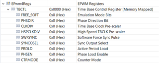
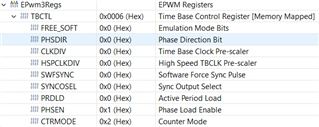
I am trying to synchronise epwm2-8 to epwm1 with each of epwm2-8 phase shifted from epwm1. The phase shift works well with epwm 1 to epwm3. From epwm 4-8, there was no phase shift even though I set this up in the code - worst enough there is a phase offset regardless of what phase shif is set for them (even at zero degree). My code is pasted below for your kind advice. In order not to bore you with annoying long script, I have limited the code to 4 modules (epwm1-4). The question now is, why are 1-3 working but 4 is not working? Result is added to show the correct phase shift between 1 and 2 (LHS). The phase offset between 1 and 4 is also added below (RHS). Two problems: (1) phase offset on epwm4-8 (2) No phase shift between epwm1 and epwm4-8 irrespective of the phase shift being set in EPwmxRegs.TBPHS.bit.TBPHS.
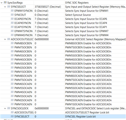
I understand that synchronisation works well with a maximum of three slaves per chain. I have tried looking into this by sychronisation scheme (below) in Figure 18-7 of the TRM - this is not helping me either. I think I am getting somethng wrong since the first chain is working correctly.


void main(void)
{
initializeVariables();
// Initialise the system control:
InitSysCtrl();
// Initialise GPIO:
InitGpio();
// Set GPIO0 and GPIO1 as ePWM1A and ePWM1B
EALLOW;
GpioCtrlRegs.GPAMUX1.bit.GPIO0 = 1; // GPIO0 = EPWM1A
GpioCtrlRegs.GPAMUX1.bit.GPIO1 = 1; // GPIO1 = EPWM1B
// Set GPIO2 and GPIO3 as ePWM2A and ePWM2B
GpioCtrlRegs.GPAMUX1.bit.GPIO2 = 1; // GPIO2 = EPWM2A
GpioCtrlRegs.GPAMUX1.bit.GPIO3 = 1; // GPIO3 = EPWM2B
// Set GPIO4 and GPIO5 as ePWM3A and ePWM3B
GpioCtrlRegs.GPAMUX1.bit.GPIO4 = 1; // GPIO4 = EPWM3A
GpioCtrlRegs.GPAMUX1.bit.GPIO5 = 1; // GPIO5 = EPWM3B
// Set GPIO6 and GPIO7 as ePWM4A and ePWM4B
GpioCtrlRegs.GPAMUX1.bit.GPIO6 = 1; // GPIO6 = EPWM4A
GpioCtrlRegs.GPAMUX1.bit.GPIO7 = 1; // GPIO7 = EPWM4B
// Set GPIO8 and GPIO9 as ePWM5A and ePWM5B
GpioCtrlRegs.GPAMUX1.bit.GPIO8 = 1; // GPIO8 = EPWM5A
GpioCtrlRegs.GPAMUX1.bit.GPIO9 = 1; // GPIO9 = EPWM5B
// Set GPIO10 and GPIO11 as ePWM6A and ePWM6B
GpioCtrlRegs.GPAMUX1.bit.GPIO10 = 1; // GPIO10 = EPWM6A
GpioCtrlRegs.GPAMUX1.bit.GPIO11 = 1; // GPIO11 = EPWM6B
// Set GPIO12 and GPIO13 as ePWM6A and ePWM6B
GpioCtrlRegs.GPAMUX1.bit.GPIO12 = 1; // GPIO12 = EPWM7A
GpioCtrlRegs.GPAMUX1.bit.GPIO13 = 1; // GPIO13 = EPWM7B
// Set GPIO15 and GPIO32 as ePWM8A and ePWM8B
GpioCtrlRegs.GPAMUX1.bit.GPIO14 = 1; // GPIO14 = EPWM8A
GpioCtrlRegs.GPAMUX1.bit.GPIO15 = 1; // GPIO32 = EPWM8B
EDIS;
// Disable CPU interrupts and clear all CPU interrupt flags:
DINT;
IER = 0x0000;
IFR = 0x0000;
// Initialize the PIE control registers to their default state.
InitPieCtrl();
// Initialize the PIE vector table with pointers to the shell Interrupt Service Routines (ISR).
InitPieVectTable();
// Map ISR function to the ePWM interrupt
EALLOW;
PieVectTable.EPWM1_INT = &epwm1_isr;
// PieVectTable.EPWM2_INT = &epwm2_isr;
// PieVectTable.EPWM3_INT = &epwm3_isr;
PieVectTable.EPWM4_INT = &epwm4_isr;
EDIS;
// Initialize ePWM modules
initEPwm1();
initEPwm2();
initEPwm3();
initEPwm4();
initEPwm5();
initEPwm6();
initEPwm7();
initEPwm8();
// Enable interrupts for ePWM1 through ePWM6 in PIEIER3
PieCtrlRegs.PIEIER3.bit.INTx1 = 1; // Enable interrupt for ePWM1
PieCtrlRegs.PIEIER3.bit.INTx2 = 1; // Enable interrupt for ePWM2
PieCtrlRegs.PIEIER3.bit.INTx3 = 1; // Enable interrupt for ePWM3
PieCtrlRegs.PIEIER3.bit.INTx4 = 1; // Enable interrupt for ePWM4
PieCtrlRegs.PIEIER3.bit.INTx5 = 1; // Enable interrupt for ePWM5
PieCtrlRegs.PIEIER3.bit.INTx6 = 1; // Enable interrupt for ePWM6
PieCtrlRegs.PIEIER3.bit.INTx7 = 1; // Enable interrupt for ePWM7
PieCtrlRegs.PIEIER3.bit.INTx8 = 1; // Enable interrupt for ePWM8
// Enable CPU INT3 which is connected to EPWM1-3 INT:
IER |= M_INT3;
// Enable CPU INT4 which is connected to EPWM4-6 INT:
IER |= M_INT4;
// Enable group 5 interrupts (ePWM7-9)
IER |= M_INT5;
// Enable global interrupts and higher priority real-time debug events:
EINT; // Enable Global interrupt INTM
ERTM; // Enable Global real-time interrupt DBGM
// IDLE loop
for(;;)
{
asm(" NOP");
}
}
void initEPwm1(void) // S1 is configured on ePWM1 module
{
//initializeVariables();
EALLOW;
// Time Base Control Register
EPwm1Regs.TBCTL.bit.CTRMODE = TB_COUNT_UPDOWN; // Count up-down mode
EPwm1Regs.TBCTL.bit.HSPCLKDIV = TB_DIV1; // High-speed time base clock pre-scaler
EPwm1Regs.TBCTL.bit.CLKDIV = TB_DIV1; // Time base clock pre-scaler
// Time Base Period Register
EPwm1Regs.TBPRD = 2400; // Set timer period
// Counter Compare Control Register
EPwm1Regs.CMPCTL.bit.SHDWAMODE = CC_SHADOW; // Enable shadow mode for CMPA
EPwm1Regs.CMPCTL.bit.SHDWBMODE = CC_SHADOW; // Enable shadow mode for CMPB
EPwm1Regs.CMPCTL.bit.LOADAMODE = CC_CTR_ZERO; // Load when counter equals zero for CMPA
EPwm1Regs.CMPCTL.bit.LOADBMODE = CC_CTR_ZERO; // Load when counter equals zero for CMPB
// Counter Compare Registers
EPwm1Regs.CMPA.bit.CMPA = 1200; // Set compare A value
EPwm1Regs.CMPB.bit.CMPB = 1200; // Set compare B value
// Action Qualifier Control Register for EPWM1A
EPwm1Regs.AQCTLA.bit.CAU = AQ_SET; // Set PWM1A on counter up equals CMPA
EPwm1Regs.AQCTLA.bit.CAD = AQ_CLEAR; // Clear PWM1A on counter down equals CMPA
// Action Qualifier Control Register for EPWM1B
EPwm1Regs.AQCTLB.bit.CBU = AQ_SET; // Set PWM1B on counter up equals CMPB
EPwm1Regs.AQCTLB.bit.CBD = AQ_CLEAR; // Clear PWM1B on counter down equals CMPB
// Dead-Band Generator Control Register
EPwm1Regs.DBCTL.bit.OUT_MODE = DB_FULL_ENABLE; // Enable Dead-band module
EPwm1Regs.DBCTL.bit.POLSEL = DB_ACTV_HIC; // Active high complementary mode
EPwm1Regs.DBCTL.bit.IN_MODE = DBA_ALL; // Dead-band input mode
// Dead-Band Rising Edge Delay Count Register
EPwm1Regs.DBRED.bit.DBRED = DT; // Dead-band rising edge delay
// Dead-Band Falling Edge Delay Count Register
EPwm1Regs.DBFED.bit.DBFED = DT; // Dead-band falling edge delay
// Master-slave synchronization
EPwm1Regs.TBPHS.bit.TBPHS = 0; // Set Phase register to zero
EPwm1Regs.TBCTL.bit.PHSEN = TB_DISABLE; // ePWM1 is master
EPwm1Regs.TBCTL.bit.PRDLD = TB_SHADOW;
EPwm1Regs.TBCTL.bit.SYNCOSEL = TB_CTR_ZERO; // Sync down-stream module
// Interrupt when TBCTR = 0
EPwm1Regs.ETSEL.bit.INTSEL = ET_CTR_ZERO;
//EPwm1Regs.ETSEL.bit.INTSEL = ET_CTR_PRD;
EPwm1Regs.ETSEL.bit.INTEN = 1; // Enable EPWM1 INT
EPwm1Regs.ETPS.bit.INTPRD = ET_1ST; // Generate interrupt on first event
EDIS;
}
void initEPwm2(void) // S2 is configured on ePWM2 module
{
//initializeVariables();
EALLOW;
// Time Base Control Register
EPwm2Regs.TBCTL.bit.CTRMODE = TB_COUNT_UPDOWN; // Count up-down mode
EPwm2Regs.TBCTL.bit.HSPCLKDIV = TB_DIV1; // High-speed time base clock pre-scaler
EPwm2Regs.TBCTL.bit.CLKDIV = TB_DIV1; // Time base clock pre-scaler
// Time Base Period Register
EPwm2Regs.TBPRD = 2400; // Set timer period (same as ePWM1)
// Counter Compare Control Register
EPwm2Regs.CMPCTL.bit.SHDWAMODE = CC_SHADOW; // Enable shadow mode for CMPA
EPwm2Regs.CMPCTL.bit.SHDWBMODE = CC_SHADOW; // Enable shadow mode for CMPB
EPwm2Regs.CMPCTL.bit.LOADAMODE = CC_CTR_ZERO; // Load when counter equals zero for CMPA
EPwm2Regs.CMPCTL.bit.LOADBMODE = CC_CTR_ZERO; // Load when counter equals zero for CMPB
// Counter Compare Registers
EPwm2Regs.CMPA.bit.CMPA = 1050; // Set compare A value (same as ePWM1)
EPwm2Regs.CMPB.bit.CMPB = 1050; // Set compare B value (same as ePWM1)
// Action Qualifier Control Register for EPWM2A
EPwm2Regs.AQCTLA.bit.CAU = AQ_SET; // Set PWM2A on counter up equals CMPA
EPwm2Regs.AQCTLA.bit.CAD = AQ_CLEAR; // Clear PWM2A on counter down equals CMPA
// Action Qualifier Control Register for EPWM2B
EPwm2Regs.AQCTLB.bit.CBU = AQ_SET; // Set PWM2B on counter up equals CMPB
EPwm2Regs.AQCTLB.bit.CBD = AQ_CLEAR; // Clear PWM2B on counter down equals CMPB
// Dead-Band Generator Control Register
EPwm2Regs.DBCTL.bit.OUT_MODE = DB_FULL_ENABLE; // Enable Dead-band module
EPwm2Regs.DBCTL.bit.POLSEL = DB_ACTV_HIC; // Active high complementary mode
EPwm2Regs.DBCTL.bit.IN_MODE = DBA_ALL; // Dead-band input mode
// Dead-Band Rising Edge Delay Count Register
EPwm2Regs.DBRED.bit.DBRED = DT; // Dead-band rising edge delay
// Dead-Band Falling Edge Delay Count Register
EPwm2Regs.DBFED.bit.DBFED = DT; // Dead-band falling edge delay
// Slave synchronization to ePWM1
EPwm2Regs.TBCTL.bit.PHSEN = TB_ENABLE; // ePWM2 is synchronized to ePWM1
EPwm2Regs.TBCTL.bit.PHSDIR = TB_DOWN;
EPwm2Regs.TBPHS.bit.TBPHS = 2100; // Phase is shift
EPwm2Regs.TBCTL.bit.SYNCOSEL = TB_SYNC_IN; // sync flow-through
// // Interrupt when TBCTR = 0
// EPwm2Regs.ETSEL.bit.INTSEL = ET_CTR_ZERO;
//// EPwm2Regs.ETSEL.bit.INTSEL = ET_CTR_PRD;
// EPwm2Regs.ETSEL.bit.INTEN = 1; // Enable EPWM1 INT
// EPwm2Regs.ETPS.bit.INTPRD = ET_1ST; // Generate interrupt on first event
EDIS;
}
void initEPwm3(void) // // S3 is configured on ePWM3 module
{
//initializeVariables();
EALLOW;
// Time Base Control Register
EPwm3Regs.TBCTL.bit.CTRMODE = TB_COUNT_UPDOWN; // Count up-down mode
EPwm3Regs.TBCTL.bit.HSPCLKDIV = TB_DIV1; // High-speed time base clock pre-scaler
EPwm3Regs.TBCTL.bit.CLKDIV = TB_DIV1; // Time base clock pre-scaler
// Time Base Period Register
EPwm3Regs.TBPRD = 2400; // Set timer period (same as ePWM1)
// Counter Compare Control Register
EPwm3Regs.CMPCTL.bit.SHDWAMODE = CC_SHADOW; // Enable shadow mode for CMPA
EPwm3Regs.CMPCTL.bit.SHDWBMODE = CC_SHADOW; // Enable shadow mode for CMPB
EPwm3Regs.CMPCTL.bit.LOADAMODE = CC_CTR_ZERO; // Load when counter equals zero for CMPA
EPwm3Regs.CMPCTL.bit.LOADBMODE = CC_CTR_ZERO; // Load when counter equals zero for CMPB
// Counter Compare Registers
EPwm3Regs.CMPA.bit.CMPA = 1400; // Set compare A value (same as ePWM1)
EPwm3Regs.CMPB.bit.CMPB = 1400; // Set compare B value (same as ePWM1)
// Action Qualifier Control Register for EPWM3A
EPwm3Regs.AQCTLA.bit.CAU = AQ_SET; // Set PWM3A on counter up equals CMPA
EPwm3Regs.AQCTLA.bit.CAD = AQ_CLEAR; // Clear PWM3A on counter down equals CMPA
// Action Qualifier Control Register for EPWM3B
EPwm3Regs.AQCTLB.bit.CBU = AQ_SET; // Set PWM3B on counter up equals CMPB
EPwm3Regs.AQCTLB.bit.CBD = AQ_CLEAR; // Clear PWM3B on counter down equals CMPB
// Dead-Band Generator Control Register
EPwm3Regs.DBCTL.bit.OUT_MODE = DB_FULL_ENABLE; // Enable Dead-band module
EPwm3Regs.DBCTL.bit.POLSEL = DB_ACTV_HIC; // Active high complementary mode
EPwm3Regs.DBCTL.bit.IN_MODE = DBA_ALL; // Dead-band input mode
// Dead-Band Rising Edge Delay Count Register
EPwm3Regs.DBRED.bit.DBRED = DT; // Dead-band rising edge delay
// Dead-Band Falling Edge Delay Count Register
EPwm3Regs.DBFED.bit.DBFED = DT; // Dead-band falling edge delay
// Slave synchronization to ePWM1
EPwm3Regs.TBCTL.bit.PHSEN = TB_ENABLE; // ePWM3 is synchronized to ePWM1
EPwm3Regs.TBCTL.bit.PHSDIR = TB_DOWN;
EPwm3Regs.TBPHS.bit.TBPHS = 2200; // Phase is shift
EPwm3Regs.TBCTL.bit.SYNCOSEL = TB_SYNC_IN; // sync flow-through
// Interrupt when TBCTR = 0
// EPwm3Regs.ETSEL.bit.INTSEL = ET_CTR_ZERO;
//// EPwm1Regs.ETSEL.bit.INTSEL = ET_CTR_PRD;
// EPwm3Regs.ETSEL.bit.INTEN = 1; // Enable EPWM1 INT
// EPwm3Regs.ETPS.bit.INTPRD = ET_1ST; // Generate interrupt on first event
EDIS;
}
void initEPwm4(void) // S4 is configured on ePWM4 module
{
//initializeVariables();
EALLOW;
// Time Base Control Register
EPwm4Regs.TBCTL.bit.CTRMODE = TB_COUNT_UPDOWN; // Count up-down mode
EPwm4Regs.TBCTL.bit.HSPCLKDIV = TB_DIV1; // High-speed time base clock pre-scaler
EPwm4Regs.TBCTL.bit.CLKDIV = TB_DIV1; // Time base clock pre-scaler
// Time Base Period Register
EPwm4Regs.TBPRD = 2400; // Set timer period (same as ePWM1)
// Counter Compare Control Register
EPwm4Regs.CMPCTL.bit.SHDWAMODE = CC_SHADOW; // Enable shadow mode for CMPA
EPwm4Regs.CMPCTL.bit.SHDWBMODE = CC_SHADOW; // Enable shadow mode for CMPB
EPwm4Regs.CMPCTL.bit.LOADAMODE = CC_CTR_ZERO; // Load when counter equals zero for CMPA
EPwm4Regs.CMPCTL.bit.LOADBMODE = CC_CTR_ZERO; // Load when counter equals zero for CMPB
// Counter Compare Registers
EPwm4Regs.CMPA.bit.CMPA = 1100; // Set compare A value (same as ePWM1)
EPwm4Regs.CMPB.bit.CMPB = 1100; // Set compare B value (same as ePWM1)
// Action Qualifier Control Register for EPWM4A
EPwm4Regs.AQCTLA.bit.CAU = AQ_SET; // Set PWM4A on counter up equals CMPA
EPwm4Regs.AQCTLA.bit.CAD = AQ_CLEAR; // Clear PWM4A on counter down equals CMPA
// Action Qualifier Control Register for EPWM4B
EPwm4Regs.AQCTLB.bit.CBU = AQ_SET; // Set PWM4B on counter up equals CMPB
EPwm4Regs.AQCTLB.bit.CBD = AQ_CLEAR; // Clear PWM4B on counter down equals CMPB
// Dead-Band Generator Control Register
EPwm4Regs.DBCTL.bit.OUT_MODE = DB_FULL_ENABLE; // Enable Dead-band module
EPwm4Regs.DBCTL.bit.POLSEL = DB_ACTV_HIC; // Active high complementary mode
EPwm4Regs.DBCTL.bit.IN_MODE = DBA_ALL; // Dead-band input mode
// Dead-Band Rising Edge Delay Count Register
EPwm4Regs.DBRED.bit.DBRED = DT; // Dead-band rising edge delay
// Dead-Band Falling Edge Delay Count Register
EPwm4Regs.DBFED.bit.DBFED = DT; // Dead-band falling edge delay
// Slave synchronization to ePWM1
EPwm4Regs.TBCTL.bit.PHSEN = TB_ENABLE; // ePWM4 is synchronized to ePWM1
EPwm4Regs.TBCTL.bit.PHSDIR = TB_DOWN;
EPwm4Regs.TBPHS.bit.TBPHS = 2250; // Phase shift from ePWM1
EPwm4Regs.TBCTL.bit.SYNCOSEL = TB_SYNC_IN; // sync flow-through
// Interrupt when TBCTR = 0
EPwm4Regs.ETSEL.bit.INTSEL = ET_CTR_ZERO;
// EPwm1Regs.ETSEL.bit.INTSEL = ET_CTR_PRD;
EPwm4Regs.ETSEL.bit.INTEN = 1; // Enable EPWM1 INT
EPwm4Regs.ETPS.bit.INTPRD = ET_1ST; // Generate interrupt on first event
EDIS;
}