This thread has been locked.

If you have a related question, please click the "Ask a related question" button in the top right corner. The newly created question will be automatically linked to this question.

TMS320F28388D: Problems with TMS320F28388D SPI

Part Number: TMS320F28388D
Other Parts Discussed in Thread: SYSCONFIG, C2000WARE, TMDSCNCD28388D

Tool/software:

Hi

I'm trying to get LS7366R iC's register value through SPI however, I have some problems with it and I need some help please cause I couldn't solve these problems for about 3 weeks ...

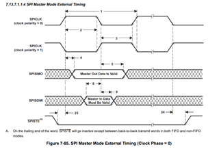
This is the SPI protocol diagram that I want to make between LS7366R(SPI slave) and TMS320F28388D(SPI master).

(This is the diagram from LS7366R datasheet. LS7366R datasheet link : https://lsicsi.com/datasheets/LS7366R.pdf

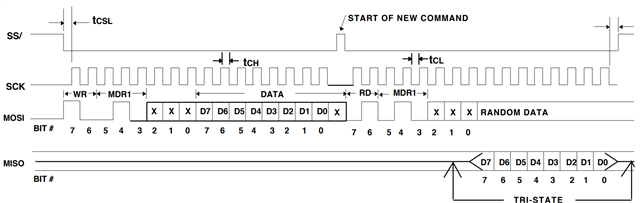
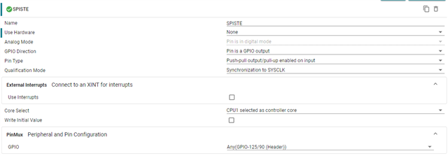
So I set my sysconfig settings, wrote the code, and connected the SPI lines to oscilloscope. These pictures are my sysconfig settings, codes, and oscilloscope signal screenshots.

//#############################################################################
//
// FILE:   spi_ex1_loopback.c
//
// TITLE:  SPI Digital Loopback
//
//! \addtogroup driver_example_list
//! <h1>SPI Digital Loopback</h1>
//!
//! This program uses the internal loopback test mode of the SPI module. This
//! is a very basic loopback that does not use the FIFOs or interrupts. A
//! stream of data is sent and then compared to the received stream.
//! The pinmux and SPI modules are configure through the sysconfig file.
//!
//! The sent data looks like this: \n
//!  0000 0001 0002 0003 0004 0005 0006 0007 .... FFFE FFFF 0000
//!
//! This pattern is repeated forever.
//!
//!  \note This example project has support for migration across our C2000 
//!  device families. If you are wanting to build this project from launchpad
//!  or controlCARD, please specify in the .syscfg file the board you're using.
//!  At any time you can select another device to migrate this example.
//!
//! \b External \b Connections \n
//!  - None
//!
//! \b Watch \b Variables \n
//!  - \b sData - Data to send
//!  - \b rData - Received data
//!
//
//#############################################################################
//
//
// $Copyright:
// Copyright (C) 2022 Texas Instruments Incorporated - http://www.ti.com
//
// Redistribution and use in source and binary forms, with or without 
// modification, are permitted provided that the following conditions 
// are met:
// 
//   Redistributions of source code must retain the above copyright 
//   notice, this list of conditions and the following disclaimer.
// 
//   Redistributions in binary form must reproduce the above copyright
//   notice, this list of conditions and the following disclaimer in the 
//   documentation and/or other materials provided with the   
//   distribution.
// 
//   Neither the name of Texas Instruments Incorporated nor the names of
//   its contributors may be used to endorse or promote products derived
//   from this software without specific prior written permission.
// 
// THIS SOFTWARE IS PROVIDED BY THE COPYRIGHT HOLDERS AND CONTRIBUTORS 
// "AS IS" AND ANY EXPRESS OR IMPLIED WARRANTIES, INCLUDING, BUT NOT 
// LIMITED TO, THE IMPLIED WARRANTIES OF MERCHANTABILITY AND FITNESS FOR
// A PARTICULAR PURPOSE ARE DISCLAIMED. IN NO EVENT SHALL THE COPYRIGHT 
// OWNER OR CONTRIBUTORS BE LIABLE FOR ANY DIRECT, INDIRECT, INCIDENTAL, 
// SPECIAL, EXEMPLARY, OR CONSEQUENTIAL DAMAGES (INCLUDING, BUT NOT 
// LIMITED TO, PROCUREMENT OF SUBSTITUTE GOODS OR SERVICES; LOSS OF USE,
// DATA, OR PROFITS; OR BUSINESS INTERRUPTION) HOWEVER CAUSED AND ON ANY
// THEORY OF LIABILITY, WHETHER IN CONTRACT, STRICT LIABILITY, OR TORT 
// (INCLUDING NEGLIGENCE OR OTHERWISE) ARISING IN ANY WAY OUT OF THE USE 
// OF THIS SOFTWARE, EVEN IF ADVISED OF THE POSSIBILITY OF SUCH DAMAGE.
// $
//#############################################################################


/*Included Files*/
#include "driverlib.h"
#include "device.h"
#include "board.h"
#include <stdio.h>


/*IR REG*/
//OP CODE
#define CLR_REG     0x00
#define RD_REG      0x40
#define WR_REG      0x80
#define LOAD_REG    0xC0

//SEL REG
#define MDR0        0x00 | (0b001 << 3)
#define MDR1        0x00 | (0b010 << 3)


/*MDR0 SETTING*/
#define MDR0_4QUAD_MODE  0x00 | 0b11

/*MDR1 SETTING*/
#define MDR1_4BYTE_MODE  0x00 | 0b00


#define STE_HIGH    GPIO_writePin(SPISTE, 1)
#define STE_LOW     GPIO_writePin(SPISTE, 0)
#define STE_STATE   GPIO_readPin(SPISTE)


/*private code*/
#define nData       2
uint16_t TxData[nData] = {0,};
uint16_t RxData[nData] = {0,};

/*Main*/
void main(void)
{
    /*start settings*/
    // Initialize device clock and peripherals
    Device_init();

    // Disable pin locks and enable internal pullups.
    Device_initGPIO();

    // Initialize PIE and clear PIE registers. Disables CPU interrupts.
    Interrupt_initModule();

    // Initialize the PIE vector table with pointers to the shell Interrupt
    // Service Routines (ISR).
    Interrupt_initVectorTable();

    // Board initialization
    Board_init();

    // Enable Global Interrupt (INTM) and realtime interrupt (DBGM)
    EINT;
    ERTM;


    /*USER CODE*/

    STE_HIGH;
    while(1)
    {
        STE_LOW;
        TxData[0] = (WR_REG | MDR0);
        TxData[1] = (MDR0_4QUAD_MODE);
        SPI_writeDataBlockingNonFIFO(mySPI0_BASE, (TxData[0] << 8U));
        SPI_writeDataBlockingNonFIFO(mySPI0_BASE, (TxData[1] << 8U));
//        DEVICE_DELAY_US(200);
        STE_HIGH;
        DEVICE_DELAY_US(20);

//        DEVICE_DELAY_US(1000);
//
//        STE_LOW;
//        SPI_writeDataBlockingNonFIFO(mySPI0_BASE, (RD_REG | MDR0) << 8U);
//        RxData[0] = SPI_readDataBlockingNonFIFO(mySPI0_BASE);
//        DEVICE_DELAY_US(20);
//        STE_HIGH;
//
//        DEVICE_DELAY_US(1000);
    }
}

//
// End File
//

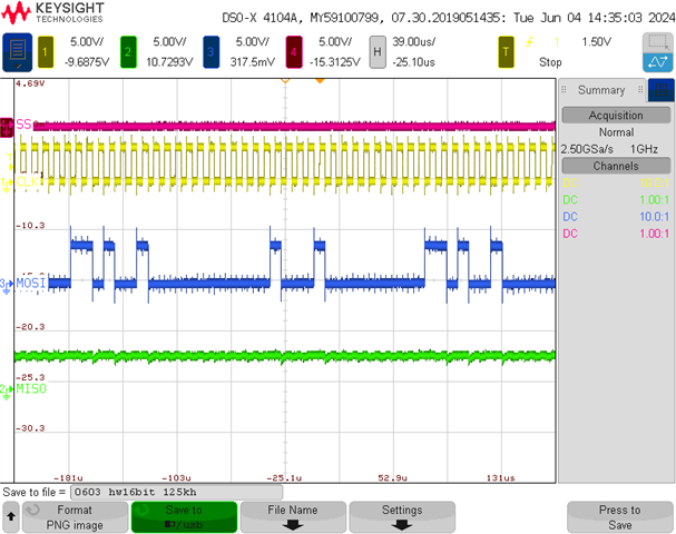
CLK should only work when STE == LOW, CLK also works when STE == HIGH.
If you look at the logic of the main code, there is absolutely no reason for CLK to work because it raises STE to HIGH after the data transmit, but I don't know why it's like this.
Looking at the oscilloscope waveform, SPI_writeDataBlockingNonFIFO and STE seem to operate independently.
Is this because of the operation of STE with GPIO? I don't know why...

In order to solve the problem of not working when the data transfer function is in the STE==LOW state, DEVICE_DELAY_US (200) was arbitrarily given between SPI_writeDataBlockingNonFIFO and STE_HIGH, and the following waveform was taken.
At this time, when looking at the STE(=SS) waveform, the LOW state is maintained exactly about 200us.

So, I wrote it in order on the code, but do GPIO and SPI move independently? How should I look at this phenomenon?
And if this is a problem caused by controlling with GPIO, how should I set it up in the SPI of sysconfig to send two 8bit data in a row?

  • Hi Sumin,

    It is indeed strange that the protocol is operating when the CS is high and might have something to do with the manual timing of the CS when using GPIOs. As a starting point, in addition to other E2Es that discuss using a GPIO as SPI, you can refer to this F2838x example that communicates with an EEPROM and controls the CS manually (C2000Ware_5_02_00_00\driverlib\f2838x\examples\c28x\spi\spi_ex6_eeprom.syscfg). Let me know if this serves to be helpful.

    Is there a specific reason you are using this GPIO implementation? If not, I would recommend using the SPIPTE pin and let the hardware takes care of the CS.

    Best Regards,
    Aishwarya

  • Hi Aishwarya Rajesh,

    I already checked the example codes from C2000 to compare with my code, however, the flow and the logic of the code was just the same as mine. (of course in my view. It might not be in other people's view.)

    And I'm using the GPIO because I need to send 2 8bit data in a row. But I could not send the data in a row when I put the CS in hardware mode.

    Are there any ways I can do it? 

  • Sumin,

    And I'm using the GPIO because I need to send 2 8bit data in a row. But I could not send the data in a row when I put the CS in hardware mode.

    Referring to C2000 SPI as well as the other SPI, it is shown that after every SPI transmission (8-16 bits), there is at least one clock cycle before the next transmission. If I am understanding correctly, you can configure the SPI to send 2 8-bits of data at a time and the hardware will take care of it going high and low accordingly. This can be put in a function that is called repeatedly. Right now, it looks like two 8-bit data are sent without taking into account the SPI rise time, hold time, setup time, etc. This information is in the datasheet and should be used to add delays which is a good approach.

    In addition, I am not sure if this will help as I haven't tested it, but have you considered setting TxData outside of the while loop since the data stays constant?

    Best Regards,

    Aishwarya 

  • Part Number: TMDSCNCD28388D

    Tool/software:

    Hi,

    I'm trying SPI communication between LS7366R iC and TI TMDSCNCD28388D board and I had a problem with CS pin software control.

    I had to control CS by software because I needed to send two 8-bit data in a row, and TI's API functions did not let that. It can only send one piece of data in one CS LOW.

    So I asked a question about my problem, and the answer I got from someone was 'try it by hardware control'.

    (my previous question: https://e2e.ti.com/support/microcontrollers/c2000-microcontrollers-group/c2000/f/c2000-microcontrollers-forum/1369140/tms320f28388d-problems-with-tms320f28388d-spi/5231435#5231435)

    To send two 8-bit data in a row, I set the SPI settings to 16-bit mode. I thought sending one 16-bit data would work the same as sending two 8-bit data.

    The code and signal shape of the result are shown below.

    /*Included Files*/
    #include "driverlib.h"
    #include "device.h"
    #include "board.h"
    #include <stdio.h>
    
    
    /*IR REG*/
    //OP CODE
    #define RD_REG      0x40
    #define WR_REG      0x80
    
    //SEL REG
    #define MDR0        0x08
    #define MDR1        0x10
    
    /*MDR0 SETTING*/
    #define MDR0_4QUAD_MODE  0x03
    
    #define STE_HIGH    GPIO_writePin(SPISTE, 1)
    #define STE_LOW     GPIO_writePin(SPISTE, 0)
    #define STE_STATE   GPIO_readPin(SPISTE)
    
    
    /*private code*/
    #define nData       2
    uint16_t TxData[nData] = {0,};
    uint16_t RxData[nData] = {0,};
    
    /*Main*/
    void main(void)
    {
        /*start settings*/
        // Initialize device clock and peripherals
        Device_init();
    
        // Disable pin locks and enable internal pullups.
        Device_initGPIO();
    
        // Initialize PIE and clear PIE registers. Disables CPU interrupts.
        Interrupt_initModule();
    
        // Initialize the PIE vector table with pointers to the shell Interrupt
        // Service Routines (ISR).
        Interrupt_initVectorTable();
    
        // Board initialization
        Board_init();
    
        // Enable Global Interrupt (INTM) and realtime interrupt (DBGM)
        EINT;
        ERTM;
    
    
        /*USER CODE*/
    
        //hardware SPI control
        TxData[0] = ((WR_REG | MDR0) << 8U) | MDR0_4QUAD_MODE;
        TxData[1] = (RD_REG | MDR0) << 8U;
    //        TxData[0] = 0x8803;
    //        TxData[1] = 0x4800;
        while(1)
        {
            HWREGH(mySPI0_BASE + SPI_O_TXBUF) = 0;
            SPI_writeDataBlockingNonFIFO(mySPI0_BASE, TxData[0]);
            DEVICE_DELAY_US(30);
    
    
            SPI_writeDataBlockingNonFIFO(mySPI0_BASE, TxData[1]);
            DEVICE_DELAY_US(30);
    
    //        RxData[0] = SPI_readDataBlockingNonFIFO(mySPI0_BASE);
    //        HWREGH(mySPI0_BASE + SPI_O_TXBUF) = 0;
    //        HWREGH(mySPI0_BASE + SPI_O_RXBUF) = {0,};
    //        HWREGH(mySPI0_BASE + SPI_O_DAT) = {0,};
        }
    }
    
    //
    // End File
    //
    

    If you look at the signal, MISO seems like it works as ACTIVE LOW, however, the default state of MISO has to be LOW.

    So I'm wondering,

    1) Why MISO acts like that?

    2) In the code I only used the SPI WRITE function. However, the SPI READ function was also activated because the MISO signal reacted. How can this be explained? 

    Also, there were some other curious outputs that I couldn't understand.

    In the code above, I tried changing the DEVICE_DELAY_US() values. When I set the delay time short, the CS pin did not act although I used the API function.

    The signal picture is below.

    I strongly think that SPICLK is somehow related to this 'delay time', but I can't guess 'what kind of relationship' there is. 

    I also tried resetting the SPI TX BUFFER at the end of the loop because I thought that it might effect on the next loop's action.

    So I wrote HWREGH(mySPI0_BASE + SPI_O_TXBUF) = 0; and the result was like the picture below.

    All I did was clearing the TX BUFFER, but the CLK acted 32 TIMES.

    How should I explain this situation? I can't analyze this result.


    PLEASE HELP ME .... 

  • you can configure the SPI to send 2 8-bits of data at a time and the hardware will take care of it going high and low accordingly.

    In the Sysconfig SPI menu, there are no such settings for data numbers.

    Also, I've checked the functions which are provided by TI, but I couldn't find such functions...

    have you considered setting TxData outside of the while loop since the data stays constant?

    I've tried this also and the result was the same.

    I put the SPI transmission function in the while loop to look at the communication signal through the oscilloscope.

  • Sumin,

    Merging threads as both threads are referring to the same question Slight smile

    I've written out steps to take to debug this issue. Hope this works for you.

    It seems like your application could use spi_ex3_external_loopback or spi_ex4_external_loopback_fifo_interrupts as a starting point.

    Taking a step back, first verify what data you are seeing (data validity). Is it consistently wrong or it is wrong on certain clock pulses? Are the clock modes of the controller and peripheral aligned? Since SPI is a duplex, synchronous module, are you reading from the RX buffer and writing to the TX buffer at the same time? Are you sending 2 8-bit data (shifted 8-bits because SPI is optimized), not 1 16-bit (this is different)?

    In terms of optimizing data writes, is it possible to use FIFO and interrupts? This would simplify your code and is pretty straightforward to use. The FIFO level can be set to 2, so after every two writes, interrupts can be used to read/write.

    Now at this point we can address the CS question: Is the requirement to have CS go high in between writes or after 2 back-to-back writes? The image attached in the original post is different than some of the comments, so I wanted to point this out again. As this screenshot from the datasheet says, it is possible do either.

    For the first option, could write one data at a time, and add a delay in between. For the second option, could write back-to-back with no delay.

    2) In the code I only used the SPI WRITE function. However, the SPI READ function was also activated because the MISO signal reacted. How can this be explained? 

    SPI modules always read and write data at the same time whether that is writing data and reading dummy data or some other combination of that.

    So I wrote HWREGH(mySPI0_BASE + SPI_O_TXBUF) = 0; and the result was like the picture below.

    SPI TX Buffer does not need to be cleared because the SPI shifts data into and out of the TX buffer automatically as long as CS is low. 

    Once again refer to the two examples linked above as a starting point as well as the SPI TRM / DS sections as it documents SPI transmission process along with the above configuration information in full detail.

    Best Regards,

    Aishwarya

  • Hi Aishwarya.
    Thank you so much for your nice comments. I appreciate it.

    Are the clock modes of the controller and peripheral aligned?

    Yes.

    Since SPI is a duplex, synchronous module, are you reading from the RX buffer and writing to the TX buffer at the same time?

    I thought I wasn't doing it because I thought that a function such as SPI_TransmitRecieve was needed for this operation.
    But in your reply, you said that,

    SPI modules always read and write data at the same time whether that is writing data and reading dummy data or some other combination of that.

    So, I think I am sending and receiving at the same time.

    Are you sending 2 8-bit data (shifted 8-bits because SPI is optimized), not 1 16-bit (this is different)?

    I am sending 2 8-bit data in the first question I wrote.
    After you told me about controlling the CS with hardware mode, I also tried sending 1 16-bit, which is my second question.

    Is the requirement to have CS go high in between writes or after 2 back-to-back writes?

    I want to write 2 8-bit data back-to-back without delay.
    And since I failed with my first code, I tried sending 1 16-bit data although I know it's different with sending 2 8-bit.

    -----------------

    I also have a few questions.

    1. What's the difference between the SPInonFIFO and SPIFIFO? Do I have to use SPI FIFO to send data back-to-back?

    2. 

    SPI modules always read and write data at the same time whether that is writing data and reading dummy data or some other combination of that.

    If so what's the difference between API functions  'SPI_writeDataBlockingNonFIFO' and 'SPI_readDataBlockingNonFIFO'?
    There must be a reason they exist regardless of acting just the same.

    3.

    In the SPI_writeDataBlockingNonFIFO function, I thought data transmission through MOSI was happening in the while loop. But now I see that while loop is just waiting for TX BUFFER to be empty, and the process of putting the data in the TX BUFFER is HWREGH(base + SPI_O_TXBUF) = data;.
    Also, HWREGH(base + SPI_O_TXBUF) = data; only puts the data in the TX BUFFER and it doesn't mean that it is shifted out through MOSI.

    Are my thoughts right?
    If so, was the reason I had to use DEVICE_DELAY_US() after I used SPI_writeDataBlockingNonFIFO() was that I had to wait for the time for the data shifting process?

    static inline void
    SPI_writeDataBlockingNonFIFO(uint32_t base, uint16_t data)
    {
        //
        // Check the arguments.
        //
        ASSERT(SPI_isBaseValid(base));
    
        //
        // Wait until the transmit buffer is not full.
        //
        while((HWREGH(base + SPI_O_STS) & SPI_STS_BUFFULL_FLAG) != 0U)
        {
        }
    
        //
        // Write data to the transmit buffer.
        //
        HWREGH(base + SPI_O_TXBUF) = data;
    }

  • Sumin,

    So, I think I am sending and receiving at the same time.

    While the SPI does automatically do that, you have to make sure you the TX/RX Buffer has the right data or dummy data (ex. don't want SPI to transmit something it shouldn't have).

    1. What's the difference between the SPInonFIFO and SPIFIFO? Do I have to use SPI FIFO to send data back-to-back?

    Primary SPI FIFO description is here, but please read the SPI TRM chapter, it has more details on the differences as well as implementation of both. You can use either mode to send data back-to-back, but I highly recommend using FIFOs, if possible.. simplifies the approach significantly.

    If so what's the difference between API functions  'SPI_writeDataBlockingNonFIFO' and 'SPI_readDataBlockingNonFIFO'?
    There must be a reason they exist regardless of acting just the same.

    Directly from comments in spi.c file:

    SPI_readDataBlockingNonFIFO - Waits for data to be received and then reads it from the buffer.
    SPI_writeDataBlockingNonFIFO - Waits for the transmit buffer to empty and then writes data to it.

    In the SPI_writeDataBlockingNonFIFO function, I thought data transmission through MOSI was happening in the while loop. But now I see that while loop is just waiting for TX BUFFER to be empty, and the process of putting the data in the TX BUFFER is HWREGH(base + SPI_O_TXBUF) = data;.
    Also, HWREGH(base + SPI_O_TXBUF) = data; only puts the data in the TX BUFFER and it doesn't mean that it is shifted out through MOSI.

    Are my thoughts right?
    If so, was the reason I had to use DEVICE_DELAY_US() after I used SPI_writeDataBlockingNonFIFO() was that I had to wait for the time for the data shifting process?

    Yes, that HWREGH line is putting data in the TX buffer. The SPI hardware shifts it out in the next clock cycle available once the TX buffer is filled based on SPI configurations. Looking at your code again, the delay is working as a temporary solution. Instead, after writing to the TX buffer twice, you need to also read the RX buffer twice. Essentially, the idea is to wait till the SPI is ready to transmit, SPI transmits data, wait till the SPI is ready to transmit, SPI transmits data, wait till SPI is ready to read, SPI reads data, wait till SPI is ready to read, SPI reads data, and repeat this process.

    Best Regards,

    Aishwarya

  • Hi Aishwarya,
    Thanks again for your reply.

    After getting your latest reply, I looked at spi_ex3_external_loopback and spi_ex4_external_loopback_fifo_interrupts.
    I thought that in the spi_ex4_external_loopback_fifo_interrupts code SPI_writeDataBlockingFIFO function would be used because it works in FIFO mode. 
    However, in this example, the API functions were not used and only private declared functions were used. I think it's because this example is more focused on the 'interrupt' and not 'FIFO'.
    So I searched for API functions that use FIFO and found SPI_transmit24Bits and SPI_pollingFIFOTransaction!
    SPI_transmit24Bits function gets 24bit data and decides it to 3 8bit data. and then, it calls SPI_pollingFIFOTransaction and this function transmits 3 8bit data to FIFO by using SPI_writeDataBlockingFIFO.

    I wanted to send 16-bit data so I had to use the SPI_transmit16Bits function however, there were only 24-bit and 32-bit transmit functions.
    So I made my function SPI_transmit16Bits_sumin that can send 16-bit data in 2 8-bit. (I named it SPI_transmit16Bits_sumin because SPI_transmit16Bits was already declared.)
    And the code I wrote for my F28388D SPI master is like this :

    /*Included Files*/
    #include "driverlib.h"
    #include "device.h"
    #include "board.h"
    #include <stdio.h>
    
    
    /*IR REG*/
    //OP CODE
    #define RD_REG      0x40
    #define WR_REG      0x80
    
    //SEL REG
    #define MDR0        0x08
    #define MDR1        0x10
    
    /*MDR0 SETTING*/
    #define MDR0_4QUAD_MODE  0x03
    
    #define STE_HIGH    GPIO_writePin(SPISTE, 1)
    #define STE_LOW     GPIO_writePin(SPISTE, 0)
    #define STE_STATE   GPIO_readPin(SPISTE)
    
    
    /*private code*/
    #define nData       2
    uint16_t TxData[nData] = {0,};
    uint16_t RxData[nData] = {0,};
    
    
    void SPI_transmit16Bits_sumin(uint32_t base, uint16_t data_1, uint16_t data_2, uint16_t txDelay);
    
    /*Main*/
    void main(void)
    {
        /*start settings*/
        // Initialize device clock and peripherals
        Device_init();
    
        // Disable pin locks and enable internal pullups.
        Device_initGPIO();
    
        // Initialize PIE and clear PIE registers. Disables CPU interrupts.
        Interrupt_initModule();
    
        // Initialize the PIE vector table with pointers to the shell Interrupt
        // Service Routines (ISR).
        Interrupt_initVectorTable();
    
        // Board initialization
        Board_init();
    
        // Enable Global Interrupt (INTM) and realtime interrupt (DBGM)
        EINT;
        ERTM;
    
    
        /*USER CODE*/
    
        //hardware SPI control
        TxData[0] = 0x0000 | (WR_REG | MDR0);      //TxData[0] = 0x0088;
        TxData[1] = 0x0000 | (MDR0_4QUAD_MODE);    //TxData[1] = 0x0003;
        SPI_transmit16Bits_sumin(SPIA_BASE, TxData[0], TxData[1], 0);


        TxData[0] = 0x0000 | (RD_REG | MDR0);      //TxData[0] = 0x0048;
    
        while(1)
        {
            SPI_transmit16Bits_sumin(SPIA_BASE, TxData[0], TxData[1], 0);
        }
    }
    
    
    void
    SPI_transmit24Bits(uint32_t base, uint32_t data, uint16_t txDelay)
    {
        uint16_t i;
        uint16_t rxBuffer[3];
        uint16_t txBuffer[3];
    
        ASSERT(data < ((uint32_t)1U << 24U));
    
        //
        // Empty Receive buffer
        //
        for(i = 0U; i < 3U; i++)
        {
            rxBuffer[i] = 0U;
        }
    
        //
        // Fill Transmit buffer with appropriate data
        //
        txBuffer[0] = (uint16_t)(data >> 16U);   // data[23:16]
        txBuffer[1] = (uint16_t)(data) >> 8U;    // data[15:8]
        txBuffer[2] = (uint16_t)(data) & 0x00FFU; // data[7:0]
    
        //
        // Three 8-bits make a 24-bit
        // Character length = 8
        // number of bytes = 3
        //
        SPI_pollingFIFOTransaction(base, 8U, txBuffer, rxBuffer, 3U, txDelay);
    }
    
    
    void
    SPI_transmit16Bits_sumin(uint32_t base, uint16_t data_1, uint16_t data_2, uint16_t txDelay)
    {
        uint16_t i;
        uint16_t rxBuffer[2];
        uint16_t txBuffer[2];
    
    //    ASSERT(data_1 < ((uint32_t)1U << 16U));
    //    ASSERT(data_2 < ((uint32_t)1U << 16U));
    
        //
        // Empty Receive buffer
        //
        for(i = 0U; i < 2U; i++)
        {
            rxBuffer[i] = 0U;
        }
    
        //
        // Fill Transmit buffer with appropriate data
        // uint32_t > uint16_t : only LOW BITs are saved.
        txBuffer[0] = (uint16_t) data_1;    // data[15:8]
        txBuffer[1] = (uint16_t) data_2; // data[7:0]
    
        //
        // Three 8-bits make a 24-bit
        // Character length = 8
        // number of bytes = 3
        //
        SPI_pollingFIFOTransaction(base, 8U, txBuffer, rxBuffer, 2U, txDelay);
    }


    //
    // End File
    //
    

    And the result was a success!!!!!
    I got the signal shape shown in the picture below.


    I'm guessing that the reason I failed with my previous code was that I wasn't using FIFO. 
    In non FIFO mode only one data transmission can be done because it only handles one data in one call of the function.

    Thank you so much for your comments. It helped me very much:)

  • Sumin,

    Glad to hear it!! Since this is a new question, can you please start a new thread with your new question (and remove it from this thread if possible)? It will be helpful to keep the content separate. I will close this thread now. Thank you.

    Best Regards,

    Aishwarya

  • Sure Aishwarya,

    I removed the new question and reposted it on the new thread!