Tool/software:
Hi,
We use the TMS320F280049C for our new project and we have the below issue for this MCU, please review the below description and provide your comment, thanks.
1. Our APP use the CLA for the power algorithm control and our C28 is used for logic operation, now, we want to update the APP program, the JTAG is well, but the SCI boot need to reset the MCU(XRSn is low);
We need to update the CLA program no need the XRSn low(Because the CLA is used for the power algorithm control and the reset will effect the power board precise);
2. The issue is the "Abnormal zero crossing drive of inverter voltage“
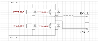
1) PWM1A and PWM1B have complementary outputs with a switching frequency of 66kHz, while PWM2A and PWM2B have complementary outputs with a switching frequency of 50Hz.
During the positive half cycle of the inverter voltage, the output of PWM2A is low, the output of PWM2B is high, and the duty cycle of PWM1A varies sinusoidally. PWM1B and PWM1A complement each other.
During the negative half cycle of the inverter voltage, the output of PWM2A is high, the output of PWM2B is low, and the duty cycle of PWM1B varies sinusoidally. PWM1A and PWM1B complement each other.

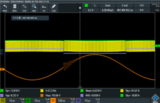
2) The orange sine wave represents the inverter voltage waveform, blue represents the PWM2A waveform, yellow represents the PWM1A waveform, and green represents the PWM1B waveform.
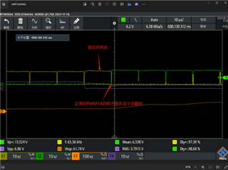
I haven't noticed any pattern of abnormal occurrences, sometimes it can occur once or twice a minute, and sometimes it doesn't occur once for tens of minutes. When an exception occurs,
the waveform of PWM2A will flip one high-frequency switching cycle ahead of schedule, or PWM1A will flip one cycle behind schedule. It is unclear who caused the delay and who caused the delay.

3) The circuit topology refer to below:

4) Our driver plesae refer to below:
a. PWM Configuration Code
EALLOW;
EPwm1Regs.TZSEL.all=0;
EPwm1Regs.TZCTL.bit.TZA = TZ_FORCE_LO; // EPWMxA will go low
EPwm1Regs.TZCTL.bit.TZB = TZ_FORCE_LO; // EPWMxB will go low
EPwm1Regs.TZFRC.bit.OST=1;
EPwm2Regs.TZSEL.all=0;
EPwm2Regs.TZCTL.bit.TZA = TZ_FORCE_LO; // EPWMxA will go low
EPwm2Regs.TZCTL.bit.TZB = TZ_FORCE_LO; // EPWMxB will go low
EPwm2Regs.TZFRC.bit.OST=1;
CpuSysRegs.PCLKCR0.bit.TBCLKSYNC = 0;
EPwm1Regs.ETSEL.bit.SOCAEN = 1; // Enable SOC on A group
EPwm1Regs.ETSEL.bit.SOCASEL= 1; // Select SOC from from CPMA on upcount
EPwm1Regs.ETPS.bit.SOCAPRD = 3; // Generate pulse on 3st event//三个开关周期触发一次采样信号
EPwm1Regs.TBPRD = 757 ; //周期
EPwm1Regs.TBPHS.bit.TBPHS=0;//设置相位
EPwm1Regs.TBCTR = 0;//计数器
EPwm1Regs.TBCTL.bit.PRDLD = TB_SHADOW;//使能影子寄存器自动重载
EPwm1Regs.TBCTL.bit.CTRMODE = TB_COUNT_UPDOWN;//向上向下计数模式
EPwm1Regs.TBCTL.bit.PHSEN=TB_DISABLE;//失能相位功能
EPwm1Regs.TBCTL.bit.PHSDIR=TB_UP;//同步后计数器向上计数
EPwm1Regs.TBCTL.bit.HSPCLKDIV = TB_DIV1;//TBCLK = EPWMCLK / (HSPCLKDIV x CLKDIV).
EPwm1Regs.TBCTL.bit.CLKDIV = TB_DIV1;
EPwm1Regs.TBCTL.bit.SYNCOSEL =TB_CTR_ZERO;//计数到0时输出同步信号
EPwm1Regs.CMPA.bit.CMPA = 1; // set duty 0% initially
EPwm1Regs.CMPCTL.bit.SHDWAMODE = CC_SHADOW;//CC_SHADOW:影子模式;CC_IMMEDIATE:立即模式
EPwm1Regs.CMPCTL.bit.LOADAMODE = CC_CTR_ZERO;//计数比较器A等于0时从影子寄存器重载值
EPwm1Regs.AQCTLA.all = 0; // set to take no action
EPwm1Regs.AQCTLA.bit.CAU = AQ_CLEAR;//向上计数时 TBCTR = CMPA 时的动作
EPwm1Regs.AQCTLA.bit.CAD = AQ_SET; //向下计数时 TBCTR = CMPA 时的动作
EPwm1Regs.AQCTLA.bit.ZRO = AQ_NO_ACTION; //TBCTR = 0的动作
EPwm1Regs.DBCTL.bit.IN_MODE = DBA_ALL;//EPWMxA 为死区模块的输入源
EPwm1Regs.DBCTL.bit.DEDB_MODE = 0;//A的上升沿延迟,B的下降沿延迟
EPwm1Regs.DBCTL.bit.POLSEL = DB_ACTV_HIC;//EPWMxA不反向,EPWMxB反向
EPwm1Regs.DBCTL.bit.OUT_MODE =DB_FULL_ENABLE;//上升沿和下降沿均延迟
EPwm1Regs.DBRED.all = 10;//上升沿延迟时钟数(死区100ns)
EPwm1Regs.DBFED.all = 10;//下降沿延迟时钟数
EPwm1Regs.CMPA.bit.CMPAHR = 0; // initialize HRPWM extension
EPwm1Regs.HRCNFG.all = 0x0;
EPwm1Regs.HRCNFG.bit.EDGMODE = HR_FEP; // MEP control on falling edge
EPwm1Regs.HRCNFG.bit.CTLMODE = HR_CMP;
EPwm1Regs.HRCNFG.bit.HRLOAD = HR_CTR_ZERO;
EPwm1Regs.HRCNFG.bit.EDGMODEB = HR_FEP; // MEP control on falling edge
EPwm1Regs.HRCNFG.bit.CTLMODEB = HR_CMP;
EPwm1Regs.HRCNFG.bit.HRLOADB = HR_CTR_ZERO;
EPwm1Regs.HRPCTL.bit.HRPE = 0; // Turn off high-resolution period
SyncSocRegs.SYNCSELECT.bit.SYNCOUT = 0;//EPWM1SYNCOUT selected to drive the SYNCOUT pin.
////EPwm2//////////////////////////////////////////////////////////////
EPwm2Regs.TBPRD = 757; // TBPRD=CPU frequency/PWM frequency/2
EPwm2Regs.TBPHS.bit.TBPHS = 0;//INV_PWM_PERIOD;//相位寄存器
EPwm2Regs.TBCTR = 0;//计数器
EPwm2Regs.TBCTL.bit.PRDLD = TB_SHADOW;//使能影子寄存器
EPwm2Regs.TBCTL.bit.CTRMODE = TB_COUNT_UPDOWN;//计数模式向上向下方式
EPwm2Regs.TBCTL.bit.PHSEN = TB_ENABLE;//TB_DISABLE;//关闭相位功能,如果使用相位寄存器,即便TBPHS=0也会延迟一个时钟周期
EPwm2Regs.TBCTL.bit.PHSDIR=TB_UP;//同步后计数器向上计数
EPwm2Regs.TBCTL.bit.HSPCLKDIV = TB_DIV1;
EPwm2Regs.TBCTL.bit.CLKDIV = TB_DIV1;
EPwm2Regs.TBCTL.bit.SYNCOSEL = TB_SYNC_IN;//同步PWM1输出的同步信号,使能相位寄存器才生效
// Counter Compare Submodule Registers
EPwm2Regs.CMPA.bit.CMPA = 1; // set duty 0% initially
EPwm2Regs.CMPCTL.bit.SHDWAMODE = CC_SHADOW;//CC_SHADOW;//计数比较器A设置为影子模式
EPwm2Regs.CMPCTL.bit.LOADAMODE = CC_CTR_ZERO;//计数比较器A等于0时从影子寄存器重载值
EPwm2Regs.AQCTLA.all=0;
EPwm2Regs.AQCTLA.bit.CAU = AQ_CLEAR;//AQ_NO_ACTION;
EPwm2Regs.AQCTLA.bit.CAD = AQ_NO_ACTION;
EPwm2Regs.AQCTLA.bit.ZRO = AQ_NO_ACTION;
// Active high complementary PWMs - Set up the deadband
EPwm2Regs.DBCTL.bit.IN_MODE = DBA_ALL;//0x0
EPwm2Regs.DBCTL.bit.DEDB_MODE = 0;
EPwm2Regs.DBCTL.bit.POLSEL = DB_ACTV_HIC;//0x2
EPwm2Regs.DBCTL.bit.OUT_MODE = DB_FULL_ENABLE;//0x3
EPwm2Regs.DBRED.all =20;//上升沿死区时钟数(200ns)
EPwm2Regs.DBFED.all =20;//下降沿死区时钟数
CpuSysRegs.PCLKCR0.bit.TBCLKSYNC = 1;
EPwm1Regs.TZCLR.bit.DCAEVT2=1;
EPwm2Regs.TZCLR.bit.DCAEVT2=1;
EPwm1Regs.TZCLR.bit.CBC=1;
EPwm2Regs.TZCLR.bit.CBC=1;
EDIS;
b. PWM driver code
EPwm1Regs.CMPA.bit.CMPA= dutyCMPA;//按正弦规律变化的占空比
EPwm2Regs.CMPA.bit.CMPA= 1;
//InvSine是0-2π正弦值
if(InvSine>=0.0f)//电压正半周
{
EPwm2Regs.AQCTLA.bit.CAU = AQ_CLEAR;
EPwm1Regs.AQCTLA.bit.CAU = AQ_CLEAR;
EPwm1Regs.AQCTLA.bit.CAD = AQ_SET;
EPwm1Regs.AQCTLA.bit.ZRO = AQ_SET;
}else{//电压负半周
EPwm2Regs.AQCTLA.bit.CAU = AQ_SET;
EPwm1Regs.AQCTLA.bit.CAU = AQ_SET;
EPwm1Regs.AQCTLA.bit.CAD = AQ_CLEAR;
EPwm1Regs.AQCTLA.bit.ZRO = AQ_CLEAR;
}


