This thread has been locked.

If you have a related question, please click the "Ask a related question" button in the top right corner. The newly created question will be automatically linked to this question.

TMS320F28379D: EMIF1 CS4 Read Verify Problem?

Part Number: TMS320F28379D


Tool/software:

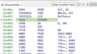
I am currently facing an issue that I have been unable to resolve. I am using EMIF1 CS4 to perform FPGA read and

write operations and to verify the program. I need assistance with this.

while(1)

        {

        fmemPtr = (uint16 *)FPGA_Start_Address;

        ESC_Value = *fmemPtr;      // EMIF1 CS4 Read 

        DELAY_US(10);

        FPGA_PWM_ON();         // EMIF1 CS4 Write

        }

#define FPGA_Start_Address    0x00380000

Using the FPGA tool, Signal Tap Logic Analyzer, as shown in the figure below.

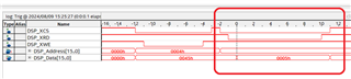
"The DSP Data Bus has an output of 0x0005, but the value cannot be found at address 0x00380000 in the DSP Memory Browser.

What other areas should I check?"

  • Hi Jordan,

    How did you connect EMIF to the FPGA device?

    The EMIF address pin EMIF_A[0] always provides the least-significant bit of a 32-bit word address. Therefore, when interfacing to a 16-bit asynchronous device, the EMIF_BA[1] pin provides the least-significant bits of the halfword or byte address. 

  • Yes, currently CS4 is connected to the FPGA for preliminary testing. When reading the address 0x380000, the value '0x0005' will be sent out for EMIF validation. Here is the hardware circuit diagram. I'm not sure if the Address Bus is defined correctly. If it is correct, what other areas need to be checked?

    //  GPIO-92 - PIN FUNCTION = --EMABA1

    GpioCtrlRegs.GPCMUX2.bit.GPIO92 = 3;

  • Hi,

    Does this schematic mean that the F28 EMIF_A0 (address 0) is connected to FPGA_A1, and F28 GPIO92 is connected to FPGA_A0?

    And data 0x45 is written to EMIF_A[15:0]=0x4 location (A2=1) --> FPGA_A[15:0] = 0x4 << 1 (first is BA[1]).

  • The screenshot you took shows the DSP performing a Write operation, In the earlier part of the program "  FPGA_PWM_ON(); 

    #define FPGA_PWM_ON() (*((Uint16 *)0x00380004)) = 0x0045, It is a " Write Cycle". My problem is " Read Cycle". I can not read data from DSP.

  • I understood. The data (0x45) is not programmed to memory.

    Please try slower EMIF clock and bigger EMIF timing parameters: setup, strobe and hold time

  • Dear Wang:

    I may have already solved the problem, but for some reason, I changed the CMD file, refreshed the CMD file, and placed some RAMGS into Page1. This allowed me to read the data at 0x380000, but some problems occurred. When executing InitFlash(), an ESTOP occurs, which didn't happen with the previous CMD file, but does occur after the modification.

    #if FLASH
    MemCopy(&RamfuncsLoadStart, &RamfuncsLoadEnd, &RamfuncsRunStart); 
    MemCopy(&Flash021_API_LoadStart, &Flash021_API_LoadEnd, &Flash021_API_RunStart); 
    InitFlash();
    #endif

    attach file CMD file

    #ifdef CLA_C
    // Define a size for the CLA scratchpad area that will be used
    // by the CLA compiler for local symbols and temps
    // Also force references to the special symbols that mark the
    // scratchpad are.
    CLA_SCRATCHPAD_SIZE = 0x100;
    --undef_sym=__cla_scratchpad_end
    --undef_sym=__cla_scratchpad_start
    #endif //CLA_C


    MEMORY
    {
    PAGE 0 : /* Program Memory */
    /* Memory (RAM/FLASH) blocks can be moved to PAGE1 for data allocation */
    /* BEGIN is used for the "boot to Flash" bootloader mode */

    BEGIN : origin = 0x080000, length = 0x000002
    RAMM0 : origin = 0x000122, length = 0x0002DE
    RAMD0 : origin = 0x00B000, length = 0x000800
    RAMLS0to5 : origin = 0x008000, length = 0x003000
    // RAMLS5 : origin = 0x00A800, length = 0x000800
    RAMGS10to15 : origin = 0x016000, length = 0x005FF8
    RESET : origin = 0x3FFFC0, length = 0x000002

    /* Flash sectors */
    FLASHA : origin = 0x080002, length = 0x001FFE /* on-chip Flash */
    FLASHB : origin = 0x082000, length = 0x002000 /* on-chip Flash */
    FLASHC : origin = 0x084000, length = 0x002000 /* on-chip Flash */
    FLASHD : origin = 0x086000, length = 0x002000 /* on-chip Flash */
    FLASHE : origin = 0x088000, length = 0x008000 /* on-chip Flash */
    FLASHF : origin = 0x090000, length = 0x008000 /* on-chip Flash */
    FLASHG : origin = 0x098000, length = 0x008000 /* on-chip Flash */
    FLASHH : origin = 0x0A0000, length = 0x008000 /* on-chip Flash */
    FLASHI : origin = 0x0A8000, length = 0x008000 /* on-chip Flash */
    FLASHJ : origin = 0x0B0000, length = 0x008000 /* on-chip Flash */
    FLASHK : origin = 0x0B8000, length = 0x002000 /* on-chip Flash */
    FLASHL : origin = 0x0BA000, length = 0x002000 /* on-chip Flash */
    FLASHM : origin = 0x0BC000, length = 0x002000 /* on-chip Flash */
    FLASHN : origin = 0x0BE000, length = 0x002000 /* on-chip Flash */
    PAGE 1 : /* Data Memory */
    /* Memory (RAM/FLASH) blocks can be moved to PAGE0 for program allocation */

    BOOT_RSVD : origin = 0x000002, length = 0x000120 /* Part of M0, BOOT rom will use this for stack */
    RAMM1 : origin = 0x000400, length = 0x000400 /* on-chip RAM block M1 */
    RAMD1 : origin = 0x00B800, length = 0x000800

    RAMGS0to4 : origin = 0x00C000, length = 0x005000
    // RAMGS4 : origin = 0x010000, length = 0x001000
    RAMGS5 : origin = 0x011000, length = 0x001000
    RAMGS6 : origin = 0x012000, length = 0x001000
    RAMGS7 : origin = 0x013000, length = 0x001000
    RAMGS8 : origin = 0x014000, length = 0x001000
    RAMGS9 : origin = 0x015000, length = 0x001000
    // RAMGS10to15 : origin = 0x016000, length = 0x005FF8
    FPGA_RAM1_1 : origin = 0x384000, length = 0x0007FF /* FPGA RAM 1.1, Store SDO object values */
    FPGA_RAM1_2 : origin = 0x384800, length = 0x0007FF /* FPGA RAM 1.2, Store SDO object ECC values */
    FPGA_RAM2 : origin = 0x385000, length = 0x000FFF /* FPGA RAM 2, Store CiA402 object values */
    FPGA_RAM3to4 : origin = 0x386000, length = 0x001FFF /* FPGA RAM 3&4, Store oscilloscope data */
    }

    SECTIONS
    {
    codestart : > BEGIN PAGE = 0, ALIGN(4)
    .text : >> FLASHB | FLASHC | FLASHD | FLASHE PAGE = 0, ALIGN(4)
    .cinit : > FLASHB PAGE = 0, ALIGN(4)
    .pinit : > FLASHB, PAGE = 0, ALIGN(4)
    .switch : > FLASHB PAGE = 0, ALIGN(4)
    .reset : > RESET, PAGE = 0, TYPE = DSECT /* not used, */
    .stack : > RAMM1 PAGE = 1
    .ebss : >> RAMGS0to4 PAGE = 1
    .esysmem : > RAMGS0to4 PAGE = 1
    .econst : >> FLASHF | FLASHG | FLASHH PAGE = 0, ALIGN(4)

    ramfuncs : LOAD = FLASHI |FLASHJ,
    RUN = RAMLS0to5,
    LOAD_START(_RamfuncsLoadStart),
    LOAD_END(_RamfuncsLoadEnd),
    RUN_START(_RamfuncsRunStart),
    RUN_SIZE(_RamfuncsRunSize),
    RUN_END(_RamfuncsRunEnd),
    PAGE = 0, ALIGN(4)

    unsecure_ramfuncs : LOAD = FLASHC,
    RUN = RAMLS0to5
    LOAD_START(_UnSecureRamfuncsLoadStart),
    LOAD_END(_UnSecureRamfuncsLoadEnd),
    RUN_START(_UnSecureRamfuncsRunStart),
    RUN_SIZE(_UnSecureRamfuncsRunSize),
    RUN_END(_UnSecureRamfuncsRunEnd),
    PAGE = 0 , ALIGN(4)

    ramfuncs
    { -l F021_API_F2837xD_FPU32.lib}
    LOAD = FLASHF,
    RUN = RAMGS10to15
    LOAD_START(_Flash021_API_LoadStart),
    LOAD_END(_Flash021_API_LoadEnd),
    RUN_START(_Flash021_API_RunStart),
    RUN_SIZE(_Flash021_API_RunSize),
    RUN_END(_Flash021_API_RunEnd),
    PAGE = 0
    /* The following section definition are for IQMATH */
    IQmath : > RAMGS0to4, PAGE=1
    IQmathTables : > RAMGS0to4, PAGE=1
    IQmathTablesRam : > RAMGS0to4, PAGE=1
    Auto_Tuning_Code : > FLASHH, PAGE = 0

    Spec_Object : > FPGA_RAM1_1, PAGE = 1
    Spec_Object_ECC : > FPGA_RAM1_2, PAGE = 1
    CiA402Bkup_Object : > FPGA_RAM2, PAGE = 1
    Oci_Scop_Buff_SEC : > FPGA_RAM3to4, PAGE = 1

    DEF_SPEC_OBJ : > FLASHK, PAGE = 0
    DEF_CIA402_OBJ : > FLASHL, PAGE = 0
    ramgs0 : > RAMGS6, type=NOINIT
    ramgs1 : > RAMGS9, type=NOINIT

    .TI.ramfunc : >> RAMGS0to4
    }

  • Hi,

    The load address and start address in your InitFlash() doesn't match the names defined in cmd file:

    MemCopy(&RamfuncsLoadStart, &RamfuncsLoadEnd, &RamfuncsRunStart); 

    MemCopy(&Flash021_API_LoadStart, &Flash021_API_LoadEnd, &Flash021_API_RunStart);