This thread has been locked.

If you have a related question, please click the "Ask a related question" button in the top right corner. The newly created question will be automatically linked to this question.

TMS320F280025: The chip does not work after power on

Part Number: TMS320F280025


Tool/software:

Dear Experts,

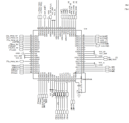
My customer encountered a situation where the chip did not work after powering on the 280025PNSR during production. The program was able to download normally, but it did not work. The measured voltage of the chip's 3.3V power supply pin was normal, and the 1.2V power supply pin was also normal. The waveform of the reset pin is shown in Figure 2. The reset delay is due to the addition of the SP809-2.9 chip, which delayed the reset by 230ms. Please help provide some suggestions for troubleshooting the abnormality. Currently, the customer has not changed the hardware and software, and some are working normally while others are abnormal

yellow is VCC_IO ;  Green is XRSN;  Blue is VCC_DSP

  • I am the user and add:
    Same board: Remove the R108, power it on, and it will work normally. (This phenomenon can be repeated) the waveform is as follows:

    yellow is VCC_IO ;  Green is XRSN;  Blue is VCC_DSP   ,Time: 5ms/ grid


  • Hello,

    The expert on this topic is currently out of office until Tuesday 9/3, so please expect a delayed response. I apologize for any inconvenience.

    Best Regards,
    Delaney

  • XRSn pin on the F28002x device is an open drain type driver(Bi-directional), so we need to connect both it and the SP809 to a external PU that will allow either to drive/release the signal.  When you remove R108 you are seeing the internal POR/BOR logic control reset exclusively, If SP809 is connected directly to the XRSn pin w/o external PU then there there will be excess current sink to our device, which may be impacting the power up.  We use a 2.2kOhm PU on our reference designs, this should work here as well.

    Also, we need to make sure the boot pins GPIO24 and GPIO32 are properly driven during boot up, which includes some time after XRSn is released(the boot ROM will sample the values on these pins to determine the boot mode).

    Best,
    Matthew

  • Thanks for your reply:
    I tested it right away,
    Replace the R108 with a 2.2kΩ resistor, but it still doesn't work.
    Leave R108 unsoldered and power it on to work.

  • In addition: For the reset pin of the 280025 chip, is it recommended to directly connect 4.7kΩ resistance to 3.3V, 100nF to GND, and nothing else?

    Is this reliable?

  • Question 1:
    Because we have mass produced, the PCB that did not work was powered on, the 0Ω resistance of R108 was removed, and the SP809 chip was disconnected from the XRSN of DSP. After testing 100 sets, all of them could work normally. Can we remove all the 0Ω resistors of R108, test and verify the functions, and then release them?
    From the current waveform from the XRSN pin, there are 2 sawtooth waves, which are reliable for product power-on start-up.

    Question 2:
    In order to ensure the reliability of the product, we arranged to test the current power on the normal work of the product, under the high temperature condition of 60℃, we tested 130 sets, working for 6 hours after the power off, and then power on, found that 8 of them could not start normally. Through this test, we should not remove the R108 resistance of all products.
    Please give us suggestions, thank you!

  • Amos,

    The connection from SP809 to the F28002x cannot be direct, there must be a common PU connection point since XRSn is a bi-directional pin from our device.  Looking back at the schematic I see there is a 4.7k PU on this net, so I'm not entirely sure why SP809 is causing an issue.  230ms is a very long time to hold off reset signal, but it should not matter. 

    Can you confirm the state of the boot pins, GPIO32/24 when XRSn goes high?  For boot to flash both these pins needs to be pulled high so the boot ROM enters the correct boot mode.  I see that GPIO24 is connected to a SPI, but GPIO32 does not connect on the image you have shown.  If these pins are not pulled up, the device could enter a different boot mode when XRSn is released.

    To you Q1, the F28002x has a built in POR/BOR logic that will hold XRSn until 3.3V rail within a certain range specified by the DS.  This should function as the supervisor, so that is why when you remove R108 you still see the device working correctly.

    As the 3.3V rail comes active there will be some transition point where the XRSn will release, the POR will get a fine trim from the eFUSE on the device, and then go back into Reset until the VDDIO reaches the final threshold.  No code will execute during this period so things should be OK from a system POV(this is why you see XRSn go high for a small amount of time then go back low before coming up high finally).

    For Q2, the device is rated to 125C, so 60C should not be an issue.  Do you know what the failure mode was for the 8 devices?  XRSn de-assert but device doesn't begin functional code or something else?  Was the device fully powered down before powering back up and XRSn goes low, etc?

    Best,
    Matthew

  • Thank you very much!

  • The current design is that GPIO24 is connected to SPI,GPIO32 does not have any connection, whether there is a weak pull up inside.
    As for the design of this, the R108 is removed, and from the current test (100 sets, continuous power on and off, can work normally), it can work normally. In this way, whether to release, flow to the customer?

    Best

    Amos

  • Amos,

    It should be OK to rely on the internal POR/BOR to gate reset.  I would advise to see if longer term you can put a pull up on GPIO32, even though there is a weak pullup we recommend to place a stronger one outside to hold the pin.

    Best,

    Matthew