This thread has been locked.

If you have a related question, please click the "Ask a related question" button in the top right corner. The newly created question will be automatically linked to this question.

TMS320F28P650DH: ADC reading issue

Part Number: TMS320F28P650DH
Other Parts Discussed in Thread: TINA-TI, SYSCONFIG, TMS320F28P659DK-Q1,

Tool/software:

Hello,

I'm trying to read the same analog signal on two different  ADC inputs.

The pin I'm using is GPIO205

I'm reading the signal on C4 and on B28.

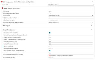
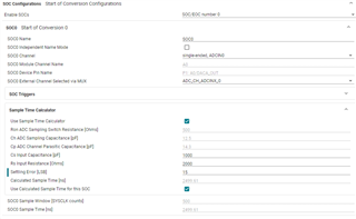
The reading is triggered by PWM1 @300KHz for both ADC, 12 bit resolution.

Both C4 and B28 return the same value.

The problem is that when I read both C4 and B28 the value is different from the case in which I read only C4.

The difference is about 20/4096 digits.

If I trigger the reading of B28 on a different pwm (PWM3, still @300KHz):

both C4 and 28 return the same value and in this case it's the same of the case in which I read only C4.

So for my application I've solved using a different trigger, but I would like to understand the reason.

Please consider also that I've also other ADC that are triggered by PWM1.

Is there a limit of ADC that I can trigger with the same PWM? Can be the issue related to the frequency?

..other limitations?

Thankyou

  • Hello,

    The expert on this topic is currently out of office until Tuesday 9/3, so please expect a delayed response. I apologize for any inconvenience.

    Best Regards,
    Delaney

  • Hello Barbara,

    If you are sampling the same signal simultaneously with two ADCs, then you need to make sure that your ADC input drive circuit is sufficiently designed to handle the sample-and-hold requirements.

    In general, the spec minimum sample-and-hold time (75ns at 12-bit resolution) assumes source impedance of < 50ohms. If your input source impedance exceeds this, you would need to calculate the required sampling window size according to the instructions in the TRM (ADC Chapter > Additional Information > Choosing an Acquisition Window Duration). The values for the sampling capacitor and series resistance are provided in the data sheet. Note that in this case, because you are sampling with two ADCs at once, the sampling capacitor value CH must be doubled. The linked application note in that TRM section also provides a TINA-TI model that can be used to simulate your input circuit design. The TI Analog Engineer's Calculator also provides a handy tool to help calculate ADC input circuit requirements.

    If a very short acquisition window is required (due to sampling rate/PWM frequency limitations), then you might need to buffer your input signal with an op amp buffer.

    Best regards,
    Ibukun

  • Hi Barbara,

    Continuing the offline conversation on this topic, which I believe was with your colleague Pietro Vacarrella.  Based from the conversation, looks like there are two variations of the input circuit.  Circuit 1 has a Thevenin's equivalent resistance of 2K and a filter cap of 1nF before the ADC input.  As Ibukun noted above, the sampling time has to be calculated according to the input impedance seen prior to the equivalent RC of the ADC input pin with its internal Ron, parasitic pin cap along with the sample and hold cap (figure 6-65 on the datasheet).  Before the analog input pin is an equivalen Rs of 2K and load cap of 1nF so the overall circuit is a two stage RC.  With the large impedances seen at the input, sampling time becomes more significant as outlined in the TRM cahpter the Ibukun pointed out.

    Alternatively, the Sysconfig tool takes care of the sampling time calculation.  This is available under SOC Configurations->Sample Time calculation.  To use the calculator, enter the equivalent Thevenin resistance as Rs and enter the input cap as below:

    You would see that there is an error since the SOC sample window holds up to a maximum count of 511 SYSCLK cycles but with the external impedances involved, it requires a much larger sampling time for a half of an LSB settling accuracy.  

    Playing along with the values, if I put a settling accuracy of around 15 LSBs then error disappears since it requires about 500 SYSCLK cycles of settling time as shown below:

    You can do the same exercise on circuit #2 if you have the equivalent Thevenin circuit on the RC network.

    Bottomline, the accuracy of conversion is largely impacted by the external impedances.  Options to consider would be reducing the external RC values of introducing a buffer/driver after the external RC to isolate the external circuit from the ADC input pin.

    Best regards,

    Joseph

  • Hello Joseph,

    we had some concerns in modeling our two circuits according to the ADC input model that is represented in your DSP datasheet, where the external driving circuit of the ADC pin is considered as an ideal voltage source Vs, a source resistor Rs and a capacitor Cs connected directly to the input pin of the ADC. Is that correct the value for Rs and Cs that we assumed for circuit 1 ? In case that there are two external RC filter in series before to go to the ADC input which is the value of Cs we have to consider ? So for example for circuit 1, we have to consider also the 10nF capacitor in some way?

    I asked Ibukun an additional point that I was not able to find in the TRM of the TMS320F28P659DK-Q1 DSP. In case of a sequence of acquisition of some analog channels on the same ADC, which is the managment of the sample and hold after the conversion of an analog channel ? The Ch capacitor is totally discharged internally before the new acquisition of the sample and hold or the Ch capacitor remains charged at the voltage of the previous sampled channel at the start of the new one ? 

    Thank you.

    Best regards.

    Pietro Vaccarella

  • Hi Pietro,

    On the first question, the Rs and Cs are whatever the ADC pin "sees" before the signals propagate to the chip, if that makes sense.

    On the second question, capacitor may not be fully discharged on the sequence of conversions if sampling time is insufficient.  Please see app note SPRACT6A specifically in the introduction on sections 1.1 ADC Input Settling and 1.2 Symptoms of Inadequate Settling.  This is important as F28P65x does not have an option to fully discharge the sampling capacitor.

    Best regards,

    Joseph

  • Hello Joseph,

    I didn't catch the first point; in case that there are two external RC filter in series before to go to the ADC input which is the value of Cs we have to consider ?

    Are correct the values that we evaluated for circuit 1 for Rs and Cs ?

    So for the second point, due to the fact that the TMS320F28P650DH haven't an active mechanism for discharging the sampling capacitor Ch after the conversion time, if I have a same trigger for two analog channels and they are associated at SOC0 and SOC1 of the same ADC-A, I can assume that at the beginning of the windows acquisition of the SOC1 the Ch capacitor is charged at the previous SOC0 voltage ?

    Thank you.

    Best regards.

    Pietro Vaccarella

  • I didn't catch the first point; in case that there are two external RC filter in series before to go to the ADC input which is the value of Cs we have to consider ?

    The model is based on the total equivalent resistance and capacitance at the ADC input pin.

    So for the second point, due to the fact that the TMS320F28P650DH haven't an active mechanism for discharging the sampling capacitor Ch after the conversion time, if I have a same trigger for two analog channels and they are associated at SOC0 and SOC1 of the same ADC-A, I can assume that at the beginning of the windows acquisition of the SOC1 the Ch capacitor is charged at the previous SOC0 voltage ?

    You can assume that the voltage on the S+H capacitor is fairly close to the previous SOC voltage.

    Best regards,
    Ibukun